World leader in customized focused ion and electron beam technology
News
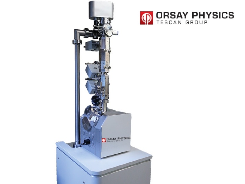
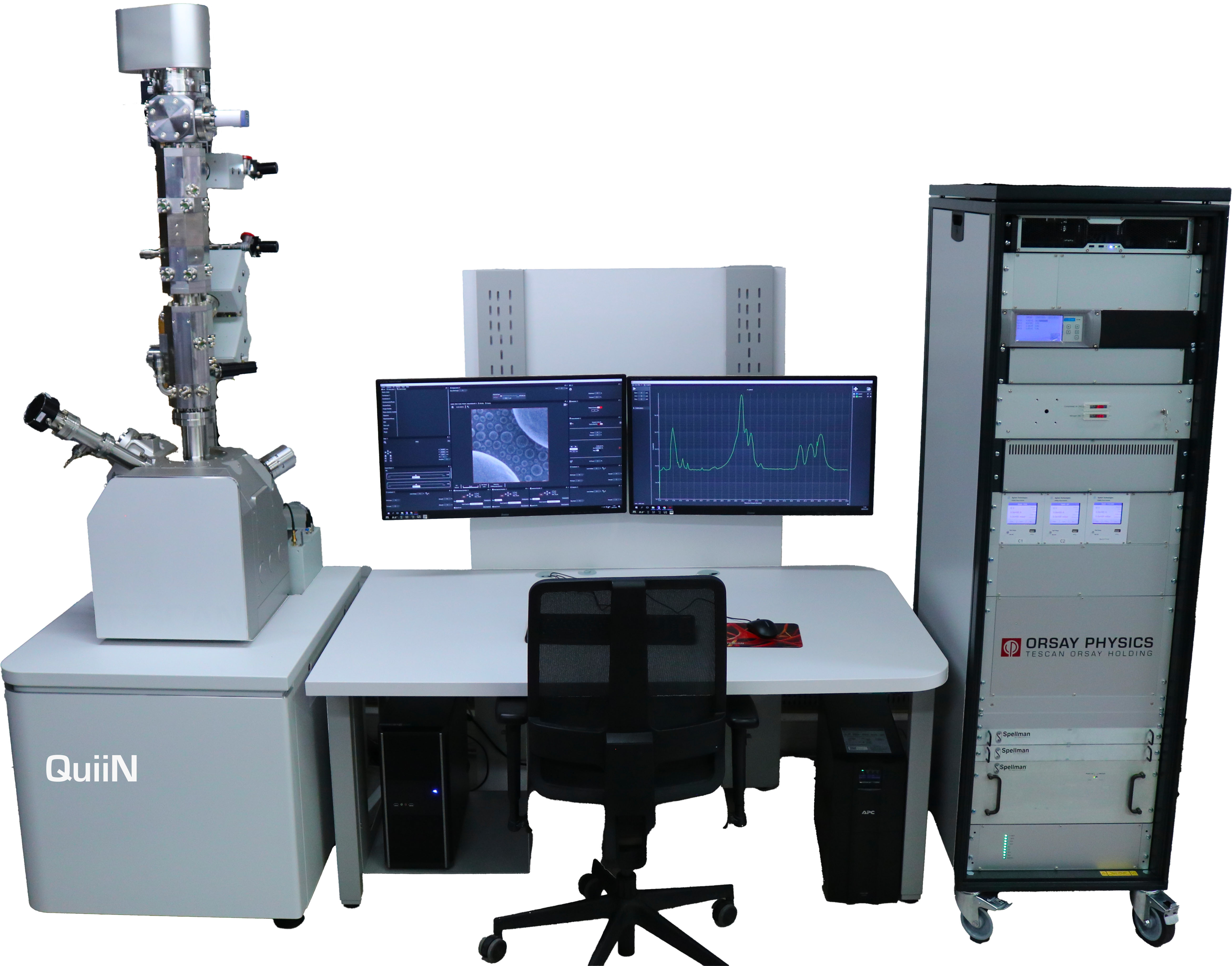
QuiiN
Precise multi - ion Implantation for discovering full spectrum of New Materials Possibilities
After the official launch during the EIPBN congress, we are proud to announce the launch of our brand-new platform, QuiiN. It represents a major advance in the field of implantation.
Discover QuiiN:
-Fine-tune and create new materials surface characteristics by unprecedented milling precision and Isotope Selection seamlessly using the Wien filter in our ion implantation tool
-Activitate dopants, repair unwanted lattice damage and immediately enhance materials properties by In-situ annealing capabilities
-Ensuring a seamless transition in your experimental setups and maximize your research efficiency with switching between specie (N, Ar, O, He, Xe or gas mixtures) or (Au, Ge, Si), all from the neutral charge
Initial feedback from our users has been extremely positive! They particularly appreciate the ease of use and efficiency of our platform.
We invite you to find out more about QuiiN and discover how it can transform your implantation applications. For more information, please contact us. Our team will be happy to answer any questions you may have.
https://www.orsayphysics.com/standalone-systems
Application Note
Chemical Nano-Characterization by Correlative Analyzes in Electron Microscopy and Secondary Ions Mass Spectroscopy: Example on Ni-Based Superalloy
The latest exciting application note from Orsay Physics: In this note, we explore the world of UHV and SIMS, presenting an application case showing an exceptional spatial resolution of 25 nm.
In this note, you'll explore:
- The incredible capabilities of our UHV technology.
- The integration of the SIMS with an electron column.
- A Ni-Based Superalloys example that demonstrates the 25 nm spatial resolution.
For scientists and researchers seeking the highest level of precision, this note is a must-read.

DeepFIB
Redefining Focused Ion Beam Technology!
We're thrilled to unveil our latest innovation – DeepFIB, the cutting-edge Gallium FIB column designed to revolutionize your applications.
DeepFIB boasts a game-changing design that's optimized for low-energy tasks and features an exceptionally focused beam, even at high currents.
Key Features:
·Maintain Ultrafine Resolution: DeepFIB ensures exceptional resolution across a wide range of current possibilities.
·Minimize Amorphization: Reduced beam energy means less amorphization during TEM lamella preparation, aligning with semiconductor technology advancements.
·High Current Mode: Experience accelerated milling with up to 135 nA, saving valuable time while preserving beam integrity.
·Seamless Integration: DeepFIB effortlessly adapts to any vacuum chamber, available in both UHV and HV configurations and capable of withstanding temperatures up to 120°C.
Explore the future of FIB technology with DeepFIB, the best FIB Gallium column on the market.
Contact us today to learn how this innovation can empower your scientific journey.

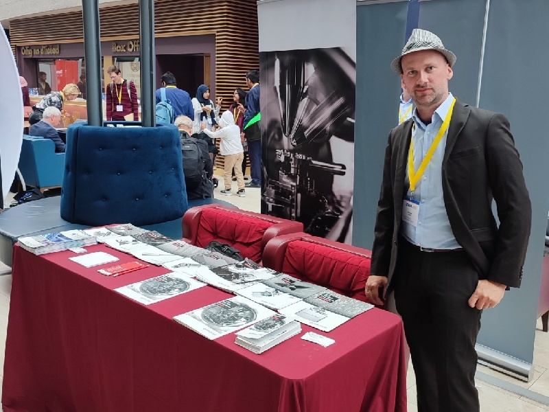
IMC20 - Busan (South Korea)
The 20th International Microscopy Congress
Orsay Physics is thrilled to announce our participation in the upcoming IMC20 Conference in Busan, South Korea from September 10th to 15th!
We're delighted to announce that Jean Almoric will be representing Orsay Physics at this prestigious event. He is bringing his expertise and passion to contribute to the scientific discourse that IMC20 offers.
Indeed, Jean will give an invited talk on Monday, September 11th, at 4:35 pm in Room 103 (division AS-01.3) He will present a new approach to correlative FIB-SEM/SIMS analysis for high-resolution imaging.
Join us as we explore revolutionary ideas, groundbreaking discoveries, and connect with fellow enthusiasts in the field. This is the perfect platform to exchange insights, forge collaborations, and stay on the cutting edge of scientific progress.
We look forward to discussing with you how our products can support your research.
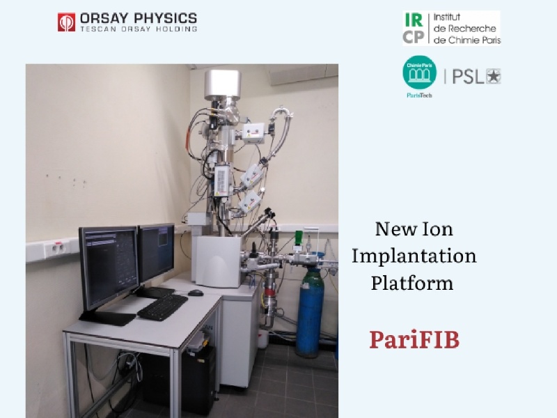
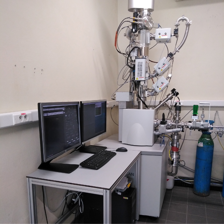
PariFIB
Color centers in diamonds are among the most promising solid-state qubit systems for the development of highly sensitive and nanoscale sensors operating at room temperature. Such color centers (including but not limited to NV, SiV, and GeV) can be created post-growth and on-demand through ion implantation in diamonds either single crystals or nanoparticles. Indeed, while in-situ doping during growth suffers from an extremely limited solubility in a tight diamond crystal lattice, as well as the difficulty to bring dopants into the gas phase, implantation enjoys a much higher flexibility in the amount, type, and spatial localization of elements that can be introduced.
Paris Sciences et Lettres (PSL University) through the engineering school Chimie-ParisTech and the CNRS laboratory IRCP (Institut de Recherche de Chimie Paris), is working on the material science developments for quantum technologies applications thanks to a program called e-DIAMANT, funded through the framework of the ANR (Agence Nationale de la Recherche) EQUIPEX+.
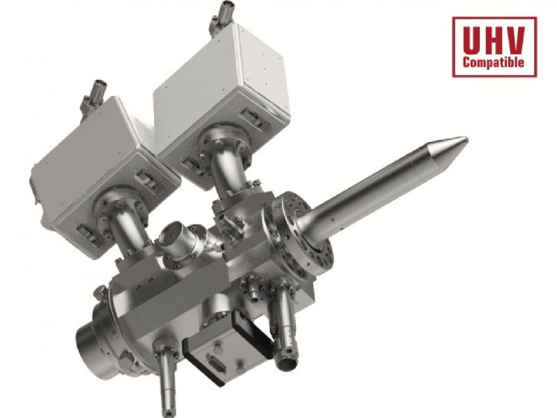
The ion implantation platform, called PariFIB, developed by Orsay Physics and installed this last month, is a versatile system allowing, among other capabilities, to create defects. Indeed, starting with undoped diamond single crystals or nanoparticles, the color centers can be directly introduced together with the associated vacancy that is created by the trace of the impinging ions. The platform integrates a filtered plasma FIB column allowing the irradiation by different gases. As a standard, N gas is used but this source can also be fueled with other gases like Xe, O, Ar or He. In addition, an in-situ annealing step to ensure an efficient creation yield either during or after the implantation can be done thanks to an in-situ heating stage, called FurnaSEM 1000. This stage, developed by Newtec, can operate under a high vacuum at a temperature of 1,000°C. Finally, a transfer interface with a load lock has been added allowing the movement of the sample from the heating stage to another chamber without exposing the sample to air.
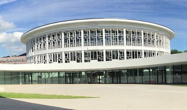
GdR-MSI - Lille (France)
Groupe De Recherche-Imagerie par Spectrométrie de Masse
Orsay Physics was present at The GdR-MSI 2023 at the Lilliad centre at the University of Lille, from Monday June 12 to Thursday June 13.
Within the GdR-MSI 2023, there were Jérémie Silvent and Jean Almoric from Orsay Physics.
During the event, Jérémie presented a Nanospace use case and explained how a FIB-SEM-SIMS analytical tool can help you understand contamination on the surface of a silicon wafer.
At this occasion, the services of TESCAN ANALYTICS will also be presented.
We look forward to discussing with you how our products can support your research.
EuFN - Zurich (Switzerland)
European FIB Network
From June 7 to 9, ORSAY PHYSICS (Jérémie Silvent and Gregory Goupil) and TESCAN GmBH andBrno, are participating in the European FIB Network (EuFN) wich will be held in Zurich (Switzerland).

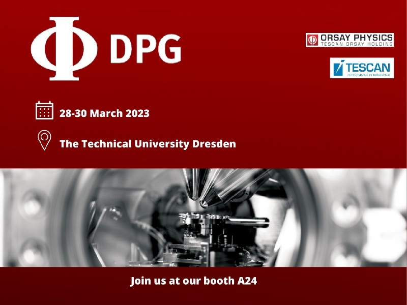
DPG - Dresden (Germany)
Deutsche Physikalische Gesellschaft - German Physical Society
From March 28 to 30, ORSAY PHYSICS and TESCAN GmBH, both subsidiaries of TESCAN ORSAY HOLDING, are participating in the Spring Meeting of condensed Matter Section of the Deutsche Physikalische Gesellschaft e. V. (DPG) wich will be held on the campus of the Technical University of Dresden (Germany).
In this context, ORSAY PHYSICS will present, among others, its Nanospace platform and its UHV FIB columns. in addition, TESCAN GmBH will showcase the various microscopes from the Tescan Orsay Holding portfolio, including the new STEM, Tensor.
Come and see us at booth A24.

NOTRE INDEX EGALITE FEMMES-HOMMES POUR L’ANNEE 2022
INDEX GLOBAL OBTENU POUR 2022 : non calculable, nos 4 indicateurs ne pouvant pas tous être calculé.
- ECART DE REMUNERATION FEMMES-HOMMES : non calculable car l’ensemble des groupes valables (c’est-à-dire comptant au moins 3 femmes et 3 hommes) représentent moins de 40% des effectifs
- ECART DE REPARTITION DES AUGMENTATIONS INDIVIDUELLES : sur la période de référence du 01/01/2022 au 31/12/2022, 15.4% des femmes ont été augmentées. Note obtenue : 35/35
- NOMBRE DE SALARIEES AUGMENTEES A LEUR RETOUR DE CONGE MATERNITE : non calculable car il n’y a pas eu de cas de retour de congé maternité pendant la période de référence.
- PARITE PARMI LES 10 PLUS HAUTES REMUNERATIONS : elles concernent 1 femme et 8 hommes. Note obtenue : 0/10
Sur l’année civile 2022 (période de référence de l’index), et compte tenu des règles de prise en compte de l’effectif, ORSAY PHYSICS part de la base suivante :
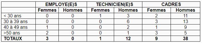
ORSAY PHYSICS, va définir en concertation avec le CSE un plan d’action mis en œuvre sur le cycle 2023-2024 pour améliorer l’égalité Femmes Hommes au sein de l’entreprise.

NOTRE INDEX EGALITE FEMMES-HOMMES POUR L’ANNEE 2021
Depuis 2020, les entreprises de plus de 50 salariés doivent calculer et publier sur leur site internet leur index de l’égalité femmes-hommes. Cet index égalité femmes-hommes se calcule en ligne à partir de l’outil EGAPRO du Ministère du Travail, de l’Emploi et de l’Insertion. Il fournit une note globale sur 100, obtenue à partir de 4 indicateurs :
- L’écart de rémunération femmes-hommes
- L’écart de répartition des augmentations individuelles
- Le nombre de salariées augmentées à leur retour de congé de maternité
- La parité parmi les 10 plus hautes rémunérations
Sur l’année civile 2021 (période de référence de l’index), et compte tenu des règles de prise en compte de l’effectif, ORSAY PHYSICS part de la base suivante :
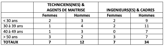
INDEX GLOBAL OBTENU : il n’a pas pu être calculable, nos 4 indicateurs n’ayant pas tous été calculables et le total obtenu étant inférieur au minimum légal de 75/100.
- ECART DE REMUNERATION FEMMES-HOMMES : non calculable car l’ensemble des groupes valables (c’est-à-dire comptant au moins 3 femmes et 3 hommes) représentent moins de 40% des effectifs (cf tableau ci-dessus)
- ECART DE REPARTITION DES AUGMENTATIONS INDIVIDUELLES : sur la période de référence du 01/01/2021 au 31/12/2021, 8 personnes ont été augmentées individuellement (hors augmentation générale) dont 1 femme. Note obtenue : 35/35
- NOMBRE DE SALARIEES AUGMENTEES A LEUR RETOUR DE CONGE MATERNITE : non calculable car il n’y a pas eu de cas de retour de congé maternité pendant la période de référence.
- PARITE PARMI LES 10 PLUS HAUTES REMUNERATIONS : elles concernent 3 femmes et 7 hommes. Note obtenue : 5/10
ORSAY PHYSICS, en concertation avec le CSE, a défini un plan d’actions mis en oeuvre d'ici mars 2023 pour améliorer l’égalité Femmes Hommes au sein de l’entreprise. Les domaines d’action choisis sont : Embauche, Santé et Sécurité au Travail, Rémunération effective, Articulation entre activité professionnelle et exercice de la responsabilité familiale.
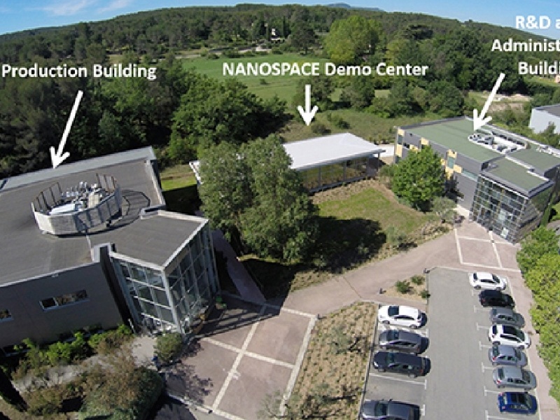
DÉCOUVERTE DES ENTITÉS DU GROUPE TESCAN À L’OCCASION DES JOURNÉES THÉMATIQUES DU GN MEBA
Lieu : NanoSpace Demo Center, Fuveau -13710

Les entités françaises du Groupe TESCAN ORSAY HOLDING vous proposent de venir découvrir leurs produits, prestations et équipes concentrés sur le site de Fuveau, le mercredi 8 juin 2022. Cette rencontre, positionnée la veille des journées thématiques du GN MEBA, sera l’occasion de vous présenter nos synergies et moyens respectifs pour répondre à vos besoins en termes d’équipements, d’études et de développement d’applications. Ainsi, vous pourrez visiter :
- TESCAN FRANCE dont la vocation est la promotion des MEB, MEB-FIB et MicroCT TESCAN
- TESCAN ANALYTICS spécialisée dans les études de caractérisation physico-chimique des surfaces et interfaces de tous types de matériaux, à partir d’un parc d’équipements de haute technologie (MEB-FIB Ga ou Xe/TEM/XPS/TOFSIMS /AFM)
- ORSAY PHYSICS entité dédiée à la conception et à la production d’équipements basés sur la physique des particules chargées (FIB, SEM, plateforme dual beams en UHV, systèmes d’injection de gaz, détecteurs,…).
Ainsi, vous pourrez visiter le NanoSpace Demo Center, et assister à la démonstration par les équipes d’ingénieurs de TESCAN France, TESCAN ANALYTICS et d’ORSAY PHYSICS des atouts de nos équipements : MEB W, MEB FEG et MEB-FIB Gallium et Plasma équipés des systèmes de microanalyse EDS-EBSD BRUKER, EDAX.
En conclusion, en une seule journée, vous pourrez découvrir :
- Notre centre de démonstration, NanoSpace Demo Center
- Le laboratoire privé Tescan Analytics
- Les moyens de conception et de production des équipements ORSAY PHYSICS
- Nos ateliers pratiques sur MEB FIB TESCAN
Selon vos besoins exprimés, nous pourrons faire évoluer le contenu des ateliers pratiques sur nos équipements, en particulier à partir de vos propres échantillons
Vous êtes intéressés, envoyez dès à présent un email à : david.barresi@tescan.com
Programme qui sera mis à jour en fonction de vos demandes particulières :
| 10h00 |
Présentation de la gamme actuelle des produits TESCAN : MEB, MEB-FIB Ga/Xe et MicroCT. |
| 09h30 | Accueil autour d’un café-croissants |
| 10h30 | Visite de TESCAN ANALYTICS : présentation de leurs offres et de leur parc d’équipements |
| 11h00 | Visite d’ORSAY PHYSICS (conception et production des colonnes FIB et GIS). |
| 12h00 |
Déjeuner |
| 13h30 |
Ateliers multiples au choix : |
| 17h00 | Discussion et fin du Workshop. |
Le programme sera mis à jour afin d’orienter les exemples d’application selon vos centres d’intérêt
ECASIA 2022 - Limerick (Ireland)
European Association on Applications of Surface and Interface Analysis
ORSAY PHYSICS and TESCAN ANALYTICS, both TESCAN ORSAY HOLDING subsidiaries, are currently participating in ECASIA 22 (29 May - 3 June, Limerick, Ireland), the 19th conference where European scientists, industrialists and equipment manufacturers meet to share their knowledge and know-how to bridge the gap between basic and applied research in surface science and to follow new trends in instrumentation. It focuses on cutting-edge scientific and technological developments in materials science/engineering, modern electronics and life sciences/biotechnology, with particular reference to surface and interface analysis. The theme of ECASIA 22 is Surface Analyses for Advanced Manufacturing.
In this context, ORSAY PHYSICS presents Nanospace, an analytical FIB SEM UHV solution, tailor made and fully customized system, equiped with a high spatially resolved SIMS. On the other hand, TESCAN ANALYTICS highlights her abilities in surface and interfaces analytical capabilities with the help of ToF SIMS (GCIB), XPS, AFM, TEM STEM EDX EELS, SEM STEM EDX EBSD, SEM-FIB Ga, Plasma FIB, ultra cryo-microtome and IRTF.
Implementation of Nanoscale Secondary-Ion Mass Spectrometry Analyses: Application to Ni-Based Superalloys
Jean Almoric,* Malik Durand, Anthony Seret, Alexis Nicolaÿ, Arnaud Houel, Isabelle Berbezier, and Nathalie Bozzolo
Secondary-ion mass spectrometry (SIMS) is probably the most widely used chemical analysis technique in semiconductor science and in metallurgy because of its ultimate sensitivity to all elements and in particular to light elements providing semiquantitative information on the depth distribution of elements, for instance, doping elements (i.e., B, H), contaminants (i.e., C and O), chemical gradients, and segregation in thin films and at interfaces, etc. With the size shrinking of systems, high-resolution 3D chemical imaging is becoming a prerequisite for the development of new materials at the nanoscale and for the deep understanding of the correlation between their properties and functionalities. Herein, the development of an innovative analytical SIMS implemented in a focused ion beam (FIB) (using Ga source)/scanning electron microscope (SEM) is reported. The equipment enables to give elemental chemical mapping at very high resolution (<30 nm) by precise optimization of the secondary-ion optics and detection, while preserving excellent sensitivity, thanks to the integration of a gas injection system(GIS), which improves a positive (negative) ionization rate with oxygen (cesium) injection. The capability of the technique is demonstrated with nanoscale characterization of Ni-based superalloys with broad applications in the manufacturing of engine parts and accessories for aircraft and aerospace equipment.
J. Almoric, I. Berbezier
Department Elaboration et MOdélisation pour les NAnotechnologies
(EMONA)
Institut Matériaux Microélectronique Nanoscience de Provence (IM2NP)
13397 Marseille, France
E-mail: jean.almoric@orsayphysics.com
J. Almoric, A. Houel
Orsay Physics
13710 Fuveau, France
M. Durand, A. Seret, A. Nicolaÿ, N. Bozzolo
Department Métallurgie, Microstructure, Rhéologie
MINES ParisTech - Centre de Mise en Forme des Matériaux (CEMEF)
06904 Sophia-Antipolis, France
The ORCID identification number(s) for the author(s) of this article can be found under
https://doi.org/10.1002/pssa.202100414. DOI: 10.1002/pssa.202100414
1. Introduction
Among the various chemical analysis techniques used routinely to determine the chemical composition of materials, there is energy-dispersive X-ray (EDX) spectroscopy implemented in a scanning electron microscope (SEM) or in a transmission electron microscope (TEM). The technique has important limitations such as the detection limit (typically above 1%), the unreliable analysis of light elements (with atomic number below Na) such as C, O, and N, and the absence of detection of He and H, making it unusable for major microelectronic and metallurgical issues. In addition, the lateral (and depth) resolution which depends on the interaction volume for X-ray generation is controlled by the accelerating voltage and the atomic number of the sample. In an SEM, the spatial and depth resolution is then of the order of 1 μm, much larger than most of the grain sizes in metallurgy for instance. In contrast, when EDX is implemented in a TEM, as the samples are thin foils (≈50 nm), the interaction volume is truncated and the electron beam crosses the sample straight on. The lateral resolution is about the beam size and the depth resolution is the sample thickness. The difficulty in this situation is the preparation of thin electron-transparent foils and the reduced field of observation (commonly few micrometers). Atom probe tomography (APT) is a chemical analysis technique recently used. APT provides a 3D elementary mapping at atomic scale with the ability to separate isotopes.[1–3] Local concentrations can be extracted from any region of the analyzed volume after reconstruction. However, the main inconveniences are first that the sample preparation commonly by focused ion beam (FIB) (as the sample should have the shape of a sharp needle with a radius smaller than 100 nm) and second that some artefacts could lead to unrealistic variations in the detected atom densities and faulty dimensions in the reconstructed volume. A strong knowledge of the sample or a correlative approach with data obtained by TEM can be used to correct these artefacts.[4–7] Recent work reports the comparison or correlation between APT and secondary-ion mass spectrometry (SIMS) techniques demonstrating the complementarityof the two chemical analysis methods.[8,9]The SIMS method is commonly used to detect trace elements and light elements due to its ultimate sensitivity. In addition, the ability to dissociate isotopes is useful in many applications as the isotope ratio can provide different information about materials. For example, tracer[10]O will give insight into oxidation or 2D tracer on mechanisms of hydrogenation in metallic superalloys.[11,12] It is based on secondary ionization after primary-ion impact, which strongly depends on the considered element and on the chemical composition of the sample. They both influence the number of secondary ions collected at each point of the sample and then the chemical distribution maps. This explains why SIMS is not quantitative, but semiquantitative, when using calibration samples. In addition, the effect of the chemical matrix on secondary ionization explains the use of reactive primary ions like oxygen or cesium. In fact, oxygen (cesium) improves positive (negative) secondary ionization,[13,14] but such ions are produced by sources of the duoplasmatron type, surface ionization sources, or plasma sources. These types of sources are not capable of producing nanometric probes (<10 nm) and this is the reason why it is difficult to obtain a resolution in chemical imaging below 50 nm with conventional SIMS.[15,16] In a conventional time-of-fight (TOF)SIMS instrument, the departure time (t0) for TOF measurement of secondary ions is provided by the pulsation of the primary-ion beam. However, the liquid metal ion sources (LMIS), widely used in SIMS, require a bunching of the primary pulse to limit its energy spreading and get a high mass resolution. (Mass resolution is measured at full width at half maximum [FWHM] of a mass peak.) However, the bunching also induces a lateral spreading of the pulse and loss of spatial resolution. A compromise between mass and spatial resolution should then be found. Recent developments allow high mass and spatial resolution, thanks to a delayed extraction, to the detriment of small mass signals that are lost.[17] The use of TOFSIMS extraction is thus unsuitable for the characterization of materials in which information on light elements, such as boron and carbon, is needed.
Instead of pulsing the primary ion beam, an orthogonal OTOFSIMS technique uses a secondary-ion pulsation to keep all benefits of high spatial resolution from the FIB without losing mass resolution.[10,18,19] In return, pulsing the secondary ions induces a duty cycle, where only part of the secondary ion beam is analyzed (from a few to about 30% depending on the mass to charge ratio and mass range). Using a magnetic sector SIMS, the mass-to-charge ratio separation is achieved through magnetic deflection instead of TOF measurement without the need for pulsing. This provides high lateral and mass resolution. Nevertheless, magnetic deflection requires one detector per mass to charge ratio, which means that a spectrometer with one detector can only detect a single element, where TOF measurement gives the entire spectrum. Nowadays, the NanoSIMS developed by Slodzian at the end of the 90 s has seven detectors,[20] and Wirtz and his team developed a magnetic sector with four detectors.[21,22] Both of these instruments are based on a double-focusing sector first developed by Mattauch et al. Even with seven detectors a magnetic sector would not be optimal to analyze a complex chemical matrix on a small region of interest (ROI); in addition, the NanoSIMS uses duoplasmatron and surface ionization sources, which limit the resolution in chemical imaging between 50 and 100nm. In this work, we present a modified O-TOFSIMS, which brings remarkable semiquantitative chemical composition at the nanoscale without demanding specific sample preparation. It appears as a promising alternative technique between APT and SEM/EDX in terms of spatial resolution and sensitivity. However, it should be noted that APT and EDX can be directly quantitative, thanks to predictive correction contrary to SIMS, which needs calibration samples for each new chemical composition study. To reach a high spatial resolution, an ultrahigh-resolution (2.5 nm) gallium FIB was used.[23,24] To overcome the low ionization rate induces by gallium, a gas injection system (GIS) was integrated on the instrument to inject oxygen, improving positive ionization rate and indirectly also improving the spatial resolution. The capabilities of the O-TOFSIMS coupled to a FIB/SEM are assessed on selected superalloy samples in terms of spatial resolution, 3D chemical imaging and spectral resolution.
2. Experimental Section
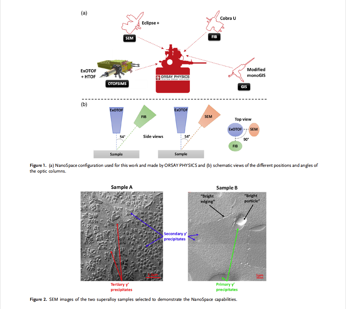
The SIMS measurements were performed using a prototypic Orsay Physics instrument, named NanoSpace, coupling OTOF SIMS and SEM, FIB, and GIS. The complete system and each of its constituents were entirely designed in-house, except for the O-TOF, to get both a high spatial resolution and a high mass resolution. The SEM column was an Eclipse Plus, and the FIB column was Cobra, equipped with a LMIS Ga source. On this FIB/SEM system, an O-TOF from Tofwerk named HTOF was integrated. The extraction column of secondary ions was completely redesigned and named ExOTOF to meet the specific mechanical constraints of the instrument and reach the best ion transmission without disturbing the primary ion beam (Figure 1).
Most of the images presented here were scanned over 9 μm2 with some of them over 5 x 5μm2. A binning was applied on the images to improve the signal-to-noise ratio at the expense of spatial resolution. For most of the images, the pixels with a size of raw data ≈5 x 5 nm2 were grouped 16 by 16 in new pixels of 20 x 20 nm2 size to improve the contrast. For this study, we selected two samples of superalloys with precipitates of various sizes and chemical compositions, allowing a good investigation of the instrument capabilities. The samples selected were Ni-based polycrystalline superalloys ref. AD730TM from Aubert & Duval company developed for turbine disk applications.[39,40] They both had a y matrix and y 0 precipitates of different sizesand natures that could be classified into three families, primary, secondary, and tertiary y 0 precipitates, denoted respectively γ’I,γ’II, and γ’III. Due to their slightly different composition but above all their thermomechanical aging, the population of these three types of precipitates differs between the two samples. In addition, we observed that two types of whitish segregations appeared after aging, which we will simply name “bright particle” for those attached to γ’I and “bright edging” for those appearing at the grain boundaries (Figure 2).
3. Results
The integration of an O-TOFSIMS in an FIBSEM system offers many capabilities, far beyond those of conventional spectrometers. First, it offers the possibility of precisely selecting the area to be analyzed such as in the examples detailed hereafter, where grain boundaries, small particles, and precipitates were accurately targeted.
Second, the correlation with SEM imaging in the backscattered mode and associated analytical techniques such as EDX and electron backscattered diffraction can lead to the strict identification of all phases, with additional precise information on phase composition, including for light elements, which is important for instance in the case of superalloys. Finally, analysis of a localized ROI is possible through in situ sample preparation by FIB in the same tool (under ultrahigh vacuum), without ex situ transfer and any risk of contamination.
The developments that we have performed focus on various parts of the NanoSpace. In a first step, a large part of the work was dedicated to the optimization of extraction and transmission of secondary ions. Transmission, denoted τ, is defined as the number of secondary ions detected per secondary ion emitted from the sample for one specie, encompassing the transmission of the various optical elements and the detection efficiency. The direct measurement of τ can be difficult but by comparison of useful yield (UY) measurements with other instruments with well-known transmission, the τ can be deduced. The UY is defined as the number of secondary ions detected per sputtered atoms of the same species. Thus, transmission and UY are linked for a considered specie A by the following equation.[13,25]
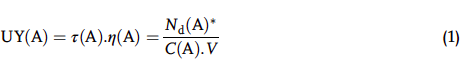
where Nd(A)* is the number of secondary ions detected of the specie A, C(A) is the concentration of the A in the sample, V is the volume sputtered, and η(A) is the ion yield defined by the number of secondary ions emitted from the surface per atom sputtered of the same specie A. η(A) depends on the chemical matrix in which the specie A is analyzed. Therefore, if particular attention is paid to the chemical matrix, a comparison of UY measurement between two different spectrometers, denoted X and Y, is possible by the following equation.
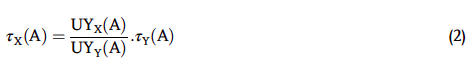
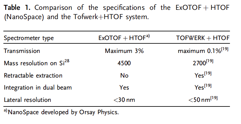
The average of four UY measurements performed in a lightly N-doped Si bulk with the ExOTOF þ HTOF system and a Ga FIB at 30 keV gives UYNS(28Si) = 2.7 x 10⁻⁶ ions atom-1. In a magnetic sector spectrometer of the type IMS 3f from CAMECA, the same measurement gives UYIMS (28Si)= 6 x 10⁻⁵ ions atom-1,[13,14] with a well-known secondary-ion transmission of 30%. The ratio of our UY measurements to that of the IMS is 22.2, applied to the IMS transmission; this gives an estimated transmission of 1.35% for our ExOTOF þ HTOF system. In the case of the OTOF technique, the duty cycle of the secondary pulsation influences the transmission, as for the same number of secondary ions emitted from the surface, fewer secondary ions will be detected. Thus, the duty cycle is a factor to be applied to the transmission of maximum 1 (100%). In our measurements, a mass range of 0—125 μ was used, which gives a duty cycle of 14% for 28Si. Depending on the mass of the secondary-ion and the mass range selected, the duty cycle varies between a few percent and just over 30% from small masses (<150 μ). The transmission of our system therefore has a maximum of 3% (Table 1).
The improvement in transmission by a factor of about 30 and an increase of about 60% in mass resolution was achieved by redesigning the secondary-ion extraction column. This is due to the fact that the Tofwerk extraction was designed as an adon. It has the advantage of being retractable and of being able to extract secondary ions at a wide angle to the sample normal. Thus, it can easily be coupled to different dual beams. ExOTOF is not retractable and must be at sample normal during SIMS analysis, but its design has been thought out, so as not to interfere with FIB/SEM applications in NanoSpace, while giving good transmission. In comparison with other types of spectrometers and even with remarkable improvement, the main drawback of the OTOF technique remains the low transmission, resulting from the duty cycle. The lateral resolution measurement was performed for both systems with a Ga LMIS having broadly the same resolution. The difference between our two measurements is explained by the difference in transmission. Indeed, to measure lateral resolution, a minimum of contrast is required and at such small scales it is often necessary to increase the size of the voxels.
In a second step, the secondary ionization yield was improved by flooding or implanting reactive elements such as oxygen and cesium. It is well known that alkalis promote negative ionization because they aim at losing one electron to reach the most stable electronic configuration like noble gases. In contrast, halogens and oxygen improve positive ionization.[14,22,26–28] As the secondary ionization yield is commonly too low for many elements to form an image at a nanometer scale, a GIS was integrated on theNanoSpace to inject Oxygen. The results with Cs will be shown in a further work.
Figure 3a demonstrates the improvement of the UY as a function of the voxel size, for the detection of silicon and germanium. The UY as defined in Equation (1) links two characteristics of SIMS, namely, detection limit and spatial resolution. For example, for a 10 nm3 voxel, a detection limit of 10% (30%) is expected for silicon (germanium), while for 10 μm3, a few tens of ppb (100 ppb) detection limit are reached. The increase in the UY indirectly increases the SIMS imaging resolution, as shown in Figure 3b. Indeed, for instance, the sixth frame image without oxygen is performed with a larger volume by voxel, leading to a loss of spatial resolution. The presence of a native oxide layer on top of most of the metals helps to enhance the secondary ionization yield during the first scans of the SIMS analyses. However, the oxide layer is not regenerated during FIB milling with a Ga source under high vacuum. The aim of O2 flooding is to create an ultrathin oxide layer between the scans. The energy of the secondary electrons (SEs) produced by collision of the Gaþ ions and the sample surface activates the reactions (following thermodynamic or kinetic laws) between the O2 adsorbed and the sample surface to form oxides.[29] Nevertheless, even if the reaction is theoretically possible, because of the competition between oxidation and FIB milling, a large surface concentration of injected gas is required to generate the reaction between the FIB scans. This is especially true, as gaseous oxygen has a poor adsorption coefficient on metal surfaces,[30,31] and then a very short landing time, making the ability to get a stationary state where both electrons and O2 are present difficult. Different oxygen flows were then tested to achieve the best secondary ionization yield, as shown in Table 2. Oxygen flow was controlled by a pressure gauge in the analysis chamber, even if it is much lower than the pressure at the surface of the sample.
Measurements presented on Table 2 show that signals of 52Crþ, 27Alþ, 48Ti+, and 58Ni+ seem optimal between 10-7 and 5.10-7mbar, leading to the choice of an oxygen pressure of ≈3.10-7mbar for the rest of this study (in comparison with 2.10-8mbar without flooding).
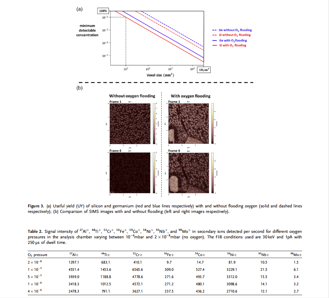
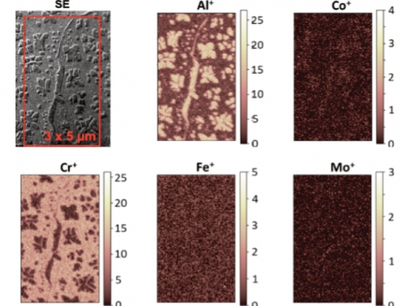
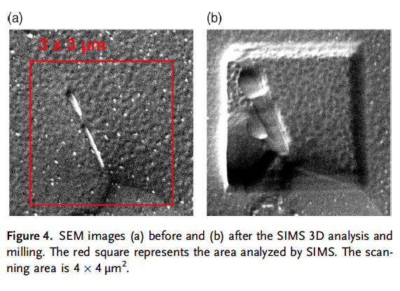
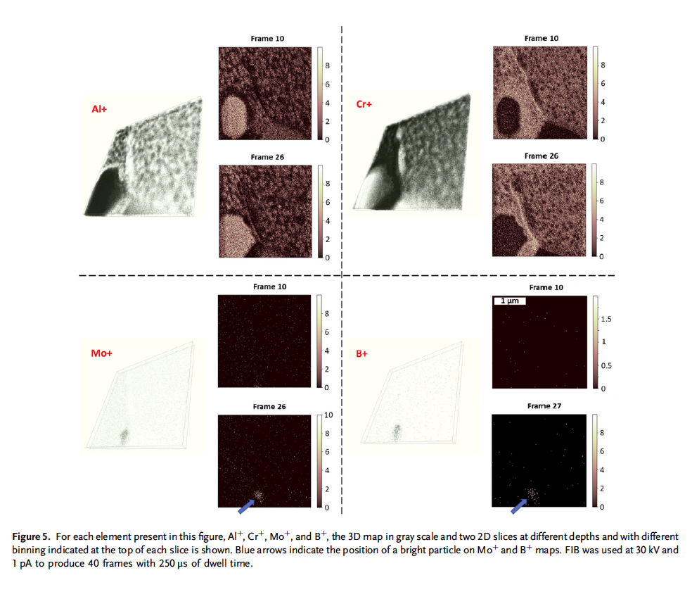
The combination of the continuous O2 flooding, a low current (1 pA), and a high number of pixels by frame (360 000) provided remarkable image quality with similar resolution for in-depth imaging as the one obtained at the surface with the native oxide (after air exposure of the sample), as shown in Figure 3b. An example of 3D SIMS imaging with O2 flooding was performed on a sample B whose SEM image is given in Figure 4. SIMS milling and 3D analyses were performed on a grain boundary with bright edging (Figure 4a). As shown in the image after milling (Figure 4b), one can observe machining allowance on the bottom of the milled area, resulting from the different milling rates (which could come from the various crystalline orientations or compositions of the grains). Inhomogeneous milling rate of polycrystalline grains is frequently observed due to the interaction of the primary beam at a fixed angle with the various orientations of the polycrystal.[32] The 3D SIMS analyse performed on the selected region highlight the presence of a =1 μm large γ’I on the Al+ and Cr+ maps (Figure 5), which is not visible at the surface on the SEM images (Figure 4a). Another smaller particle of different compositions (mainly B and Mo) that is not visible in the SEM images either is revealed on the chemical maps (blue arrows) in Figure 5. By comparing the images frame by frame from the beginning of the milling, it is clear that this particle was not present on the top surface of the sample. In addition, the presence of Mo and B suggests that it could be a bright particle like the ones observed on the SEM image of sample B (Figure 2).
Thanks to the oxygen flooding, γ’’II (<100 nm) are clearly visible on all the Al+ and Cr+ maps, from the top surface to in depth of the alloy (at about 200 nm depth), as shown in Figur 5. The white line visible in the SEM image in Figure 4a was not visualized on any of the chemical maps (Figure 5). This is explained by its very low milling rate as compared with the other components of the sample (precipitates and matrix); it is also consistent with its appearance as a protrusion on the SEM image after milling (Figure 4b). In a third set of experiments, we optimized the FIB experimental parameters to improve the imaging resolution. First, a compromise was found to optimize the TOF period as on one side, the TOF period should be as low as possible to improve the duty cycle. Indeed, the abrasion is continuous during the pulse of secondary ions and the reduction of its duration permits to increase the part of secondary ions analyzed. On the other side, the TOF period must be long enough to accommodate the heaviest masses to be detected. In our experimental conditions, the heaviest element is tungsten with a TOF of 24.1 μs for its highest isotope. For this reason, the TOF period was set to 25 μs.
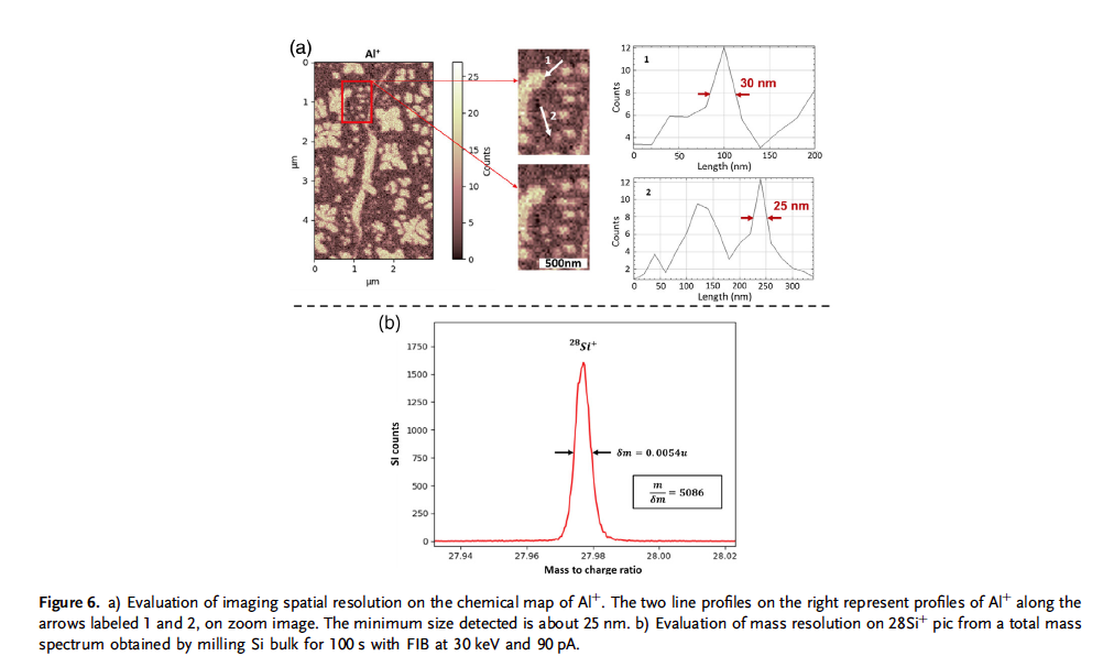
The energy of the primary beam was set to its maximum value (30 keV) to reduce the chromatic aberration and maximize the lateral resolution of the ion beam. In addition, the beam current was set to 1 pA, which is the result of the high magnification obtained using the condenser lens and the selection of the smallest possible aperture to reduce the opening angle. The high magnification and low aperture angle reduce theGaussian and spherical terms, respectively, resulting in the smallest probe diameter.[33,34] Thanks to these optimizations, a resolution below 5 nm was reached for the SE image made from a primary-ion beam tilted at 55.
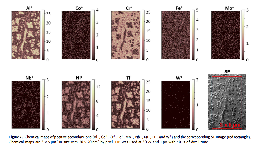
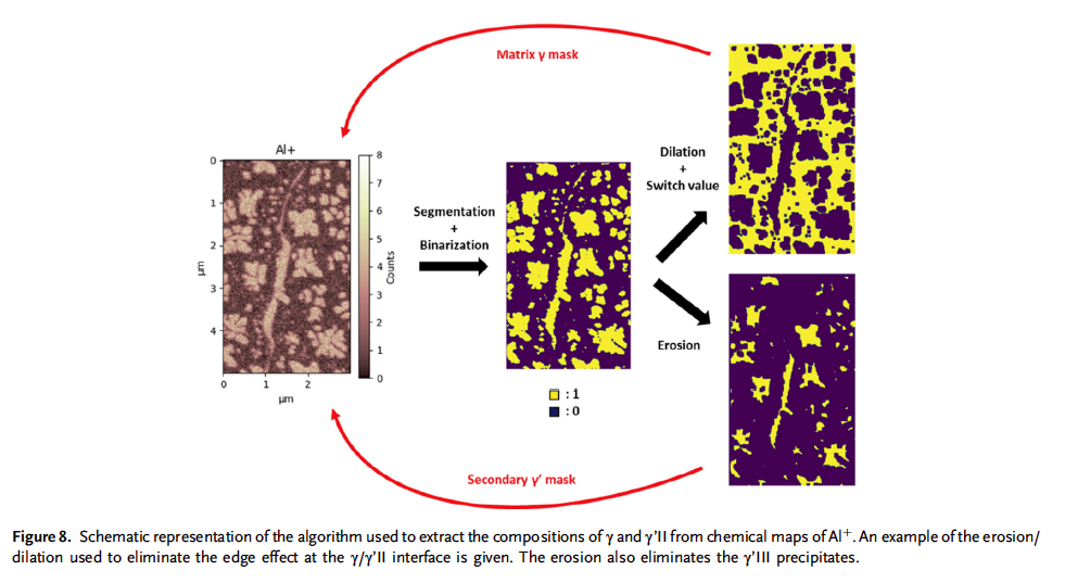
To determine the spatial resolution, three 16/84 measurements were performed using the “GaussFit” plugin of image J. That means that the derivative of a slope was measured between 16% and 84% of the slope formed by the convolution between the ionic probe and an edge,[15] such as an interface γ’/γ’Il in our case. These measurements were done in three different directions of the Alþ maps. A resolution about 23 nm never achieved before with a Ga FIB and/or an O-TOF was reached. An example of line profile with 25 nm resolution on a γ’’II is given in Figure 6a. In addition, thanks to the secondary-ion beam pulsation (instead of the primary pulsation of conventional TOFSIMS), a mass resolution of at least 4500 was routinely obtained on 28Si (Figure 6b). The mass resolution is defined as the mass divided by the FWHM of its peak. The high mass resolution of NanoSpace enables the separation of isotopes in the mass spectrum and even the dissociation of mass overlap induced by hydrides. Therefore, the accumulation of isotopes intensity is possible without mass interference. Chemical maps of positive secondary ions from the nine elements identified above are shown in Figure 7. First, it should be noted from Figure 7 that some of the chemical maps evidence a large contrast, which clearly distinguishes the γ’II and γ’III precipitates from the surrounding matrix, while other maps have almost no contrast. This difference is explained either by a different ionization rate (for instance, metals like Al, Cr, and Ti have a higher ionization rate than Co, Ni, Nb, and Mo[35–37]) or by the composition and the compositional variations between the matrix and the precipitates. In the case of W, it is even more difficult to get any signal at this submicrometric scale, as it has both the poorest ionization yield and the lowest concentration. Second, even if the maps of Al, Cr, Ni, and Ti clearly distinguish the γ’II and γ’III precipitates from the surrounding matrix, it remains difficult to quantify their concentration from SIMS data without a calibration sample. Indeed, there is no sufficiently reliable theoretical model to predict the ionization yield of a species in a given chemical matrix. It is then highly challenging to calibrate the SIMS measurements to get semiquantitative analysis. For simplicity of comparison between different SIMS analysis, the focus is placed on the composition ratio between the γ’II precipitates and the γ matrix. To reduce the statistical error made on the number of secondary ions collected, it is necessary to have as much information as possible on both phases. For this, a segmentation algorithm was used to separate the two phases in each image. The algorithm is a version of the Chan-Vese algorithm using morphological operators instead of solving a partial differential equation of the evolution of the contour.[38] This algorithm, described in Figure 8, consists of using an image with a good contrast/resolution compromise, for instance, for Al mapping, we use a binning of two.
The segmentation binarizes the image, which provides a mask that can be multiplied by the mappings of each element to obtain the number of secondary ions detected per element in the γ’II precipitates. The mask for the γ matrix can be obtain by inverting the values of the γ’II mask. The edge effects at the γ/γ’II interfaces are eliminated using morphological dilation (erosion) for the γ (γ’II) mask. Morphological dilation (erosion) applies the value of a pixel in (i, j), when it is at the maximum (minimum) on all the pixels of the neighborhood centered in (i, j). The radius of the neighborhood is determined in our case by the imaging resolution (5 pixels). Dilation (erosion) enlarges bright (dark) regions and shrinks dark (bright) regions. The erosion was deliberately more pronounced (8 pixels) to exclude tertiary γ’II precipitates.
.
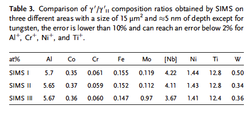
The reliable protocol implemented here allows to quantify the information of the two phases. Its reproducibility is testified by the different measurements performed in different positions of the sample, that demonstrate an error lower than 10% for all elements except for tungsten. Indeed, the combination of a low concentration and a very low ionization rate of tungsten gives a high error close to 35% in this measurement, but it can be overcome by milling a larger volume (here at about 0.075μm3). In contrast, the error is below 2%for Al+, Cr+, Ni+, and Ti+, as shown in Table 3, where the γ’II/γ concentration ratios obtained by SIMS in three different regions in 30s for each are given. In a last step, corrective factors must be applied to account for matrix effects (e.g., using APT values) and the sample can be used as a standard for chemical characterization of other Ni-based superalloys at a scale <30nm. Beyond Ni-based superalloys, this semiquantification protocol can be used on other types of solid materials exhibiting different phases to characterize the chemical composition of these phases. For example, in metallurgy, other types of metal alloys have small precipitates and their chemical characterization allows a better understanding of the nucleation and growth mechanisms of these precipitates, and thus it can help to predict the macroscopic mechanical characteristics of these alloys. It should be noted that for each study on a new material, the SIMS measurement should be properly calibrated with a standard sample or by another technique which is quantitative.”
4. Conclusion
We have reported the development of a modified O-TOFSIMS which brings remarkable semiquantitative chemical composition at the nanoscale without demanding specific sample preparation. The integration of a GIS allows the flooding of the samples surface with oxygen during SIMS analysis, increasing significantly the positive secondary ionization. The capabilities of O-TOFSIMS coupled to a high-resolution Ga-based FIB/SEM are assessed on Ni-based superalloy samples. Despite a low transmission (<3%), chemical maps at the nanoscale were obtained, where y’III precipitates with a size < 30nm were detected and imaged. This high lateral resolution was obtained without degrading the high mass resolution of 4500 routinely obtained on 28Si. Localized chemical analyses of specific features at the grain boundaries and on segregated areas are also reported. In addition, a correlative analysis between SEM/EDX and SIMS imaging addresses some remaining questions about the chemical maps obtained. A segmentation protocol was developed to isolate the various chemical phases on very small volumes (<0.1 μm3). The reliability of the semiquantification process is demonstrated.
Acknowledgements
The authors are very grateful to Orsay Physics for financial support. The authors also thank Dr. Serge Della Negra (IPNO) for his scientific and technical support on SIMS technique.
Conflict of Interest
The authors declare no conflict of interest.
Data Availability Statement
Data available on request from the authors.
Keywords
focused ion beam, nanoscale characterizations, Ni-based superalloys, orthogonal time of flight, scanning electron microscopy, secondary-ion mass spectrometry
Received: June 29, 2021
Revised: October 16, 2021
Published online:
[1] D. Blavette, A. Bostel, J. M. Sarrau, B. Deconihout, A. Menand, Nature 1993, 363, 432.
[2] D. Blavette, F. Vurpillot, B. Deconihout, Tech. l’ingénieur Anal. Surf. Matériaux 2013, P900, v21.
[3] D. Blavette, A. Menand, Tech. l’ingénieur. Anal. Caractér. 1995.
[4] D. Melkonyan, C. Fleischmann, L. Arnoldi, J. Demeulemeester, A. Kumar, J. Bogdanowicz, F. Vurpillot, W. Vandervorst, Ultramicroscopy 2017, https://doi.org/10.1016/j.ultramic.2017.04.006.
[5] A. Kirchmayer, H. Lyu, M. Pröbstle, F. Houllé, A. Förner, D. Huenert, M. Göken, P. J. Felfer, E. Bitzek, S. Neumeier, Adv. Eng. Mater. 2020, 22, 2000149.
[6] C. Hatzoglou, B. Radiguet, G. Da Costa, P. Pareige, M. Roussel, M. Hernandez-Mayoral, C. Pareige, J. Nucl. Mater. 2019, 522, 64.
[7] M. Herbig, P. Choi, D. Raabe, Ultramicroscopy 2015, 153, 32.
[8] E. Kautz, J. Cliff, T. Lach, D. Reilly, A. Devaraj, Analyst 2021, 146, 69.
[9] Z. Wang, J. Liu, Y. Zhou, JJ. Neeway, D. K. Schreiber, J. V. Crum, J. V. Ryan, X. L. Wang, F. Wang, Z. Zhu, Surf. Interface Anal. 2016, 48, 1392.
[10] D. S. Selby, V. Mlynski, M. Guilhaus, Int. J. Mass Spectrom. 2001, 89.
[11] F. B. Ismail, V. A. Vorontsov, T. C. Lindley, M. C. Hardy, D. Dye, B. A. Shollock, Corros. Sci. 2017, 116, 44.
[12] Y. Aboura, K. L. Moore, Appl. Surf. Sci. 2021, 557, 149736.
[13] M. Schuhmacher, H. N. Migeon, B. Rasser, Conf. Proc. SIMS VIII 1991.
[14] G. Frache, B. El. Adib, J. N. Audinot, H. N. Migeon,, Surf. Interface Anal. 2011, 43, 639.
[15] J. Zhang, Y. Lin, W. Yang, W. Shen, J. Hao, J. Anal. At. Spectrom. 2014, 29, 1934.
[16] K. Li, J. Liu, C. R. M. Grovenor, K. L. Moore, Annu. Rev. Anal. Chem. 2020, 13, 273.
[17] Q. P. Vanbellingen, N. Elie, M. J. Eller, S. Della-Negra, D. Touboul, A. Brunelle, Rapid Commun. Mass Spectrom. 2015, 29, 1187.
[18] J. H. J. Dawson, M. Guilhaus, Rapid Commun. Mass Spectrom. 1989, 3, 155.
[19] L. Pillatsch, F. Östlund, J. Michler, Prog. Cryst. Growth Character. Mater. 2019, 65, 1.
[20] F. J. Stadermann, R. M. Walker, E. Zinner, Meteorit. Planet. Sci. 1999, 34, A111.
[21] T. Wirtz, D. Dowsett, P. Philipp, J. N. Audinot, S. Eswara Moorthy, Microsc. Microanal. 2015, 21, 2319.
[22] T. Wirtz, P. Philipp, J. N. Audinot, D. Dowsett, S. Eswara, Nanotechnology 2015, 26, 434001.
[23] S Guillous, C Bourin, B Ban D’Etat, A Benyagoub, A Cassimi, C Feierstein, E Gardés, E Giglio, S Girard, C Grygiel, A Houel, H Lebius, A Méry, I Monnet, J-M Ramillon, J Rangama, F Ropars, E Verzeroli, M Viteau, A Delobbe, Rev. Sci. Instrum. 2016, 87, 113901.
[24] L. Bischoff, P. Mazarov, J. Giearak, L. Bruchhaus, Appl. Phys. Rev. 2016, 3, 021101.
[25] L. Li, D. S. McPhail, N. Yakovlev, H. Seng, Surf. Interface Anal. 2011, 43, 495.
[26] P. Philipp, T. Wirtz, H. N. Migeon, H. Scherrer, Appl. Surf. Sci. 2006, 252, 7205.
[27] A. Priebe, I. Utke, L. Pethö, J. Michler, Anal. Chem. 2019, 91, 11712.
[28] K. Franzreb, P. Williams, Surf. Interface Anal. 2011, 43, 129.
[29] I. Utke, S. Moshkalev, P. Russell, in Nanofabrication Using Focused Ion And Electron Beams: Principles And Applications (Eds: I. Utke,
S. Moshkalev, P. Russell), Oxford Univ. Press, Oxford, UK 2012, pp. 126–183.
[30] A. Winkler, K. D. Rendulic, K. Wendl, Appl. Surf. Sci. 1982, 14, 209.
[31] H. P. Bonzel, R. Ku, Surf. Sci. 1973, 40, 85.
[32] C. A. Volkert, A. M. Minor, MRS Bulletin 2007, 32, 389.
[33] J. Orloff, Rev. Sci. Instrum. 1993, 64, 1105.
[34] J. Orloff, L. W. Swanson, M. Utlaut, J. Vac. Sci. Technol. B Microelectron. Nanom. Struct. 1996, 19, 2533.
[35] A. Laufer, S. Eisermann, N. Volbers, K. Potzger, S. Geburt, C. Ronning, J. Appl. Phys. 2011, 110.
[36] F. A. Stevie, R. G. Wilson, J. Vac. Sci. Technol. A Vacuum, Surfaces, Film. 1991, 9, 3064.
[37] R. G. Wilson, S. W. Novak, J. Appl. Phys. 1991, 69, 466.
[38] P. Marquez-Neila, L. Baumela, L. Alvarez, IEEE Trans. Pattern Anal. Mach. Intell. 2014, 36, 2.
[39] A. Devaux, E. Georges, P. Héritier, in Superalloy 718 and Derivatives (Eds: E. A. Ott, J. R. Groh, A. Banik, I. Dempster, T. P. Gabb, R. Helmink, X. Liu, A. Mitchell, G. P. Sjöberg, A. Wusatowska-Sarnek), Springer 2010, pp. 222–235, https://doi.org/10.1002/9781118495223.ch16.
[40] A. Devaux, E. Georges, P. Héritier, Adv. Mater. Res. 2011, 278, 405.
RECRUTEMENT EN CDI D'UN(E) RESPONSABLE RESSOURCES HUMAINES
belle opportunité pour une personne ayant une expérience des PME/ETI
CONTEXTE :
Nos activités de recherche et développement comme de production concentrent 80% de nos ressources humaines comme matérielles. S’il est essentiel pour nous de concevoir des équipements de haute technologie, complexes, dédiés et innovants, il n’en est pas moins vital d’être en mesure de les produire de façon répétitive, personnalisée et fiable. Cette production concerne des petites et moyennes séries de produits sensibles, expédiés aux quatre coins du monde, majoritairement pour des grands groupes industriels internationaux. Par ailleurs, compte tenu de notre relative petite taille par rapport à nos concurrents, la réactivité, la flexibilité et la qualité de la relation client font parties de nos atouts essentiels. Compte tenu de ces particularités, nos équipes (près de 70 personnes), sont constituées de personnes de niveau de formation allant du CAP à BAC+8 ou plus, avec en production majoritairement des « hommes de l’art » bénéficiant d’une grande expérience et de réels savoir-faire, ainsi que des scientifiques et ingénieurs spécialisés en R&D. Les technologies mises en œuvre, ainsi que les attentes de nos clients, nécessitent beaucoup de concentration, d’efficacité et de synergies de la part de tout notre personnel.
DESCRIPTION DE LA FONCTION :
Rattachée à la Direction Générale, la personne aura pour principales missions :
Ø Effectuer et assurer le suivi des activités liées aux ressources humaines :
- Recrutement et intégration de nouveaux arrivants, gestion des sortants : majoritairement des CDI, mais aussi des CDD, thésards, alternants, stagiaires, personnels mis à disposition
- Pilotage campagnes d’entretiens d’évaluation et professionnels
- Mise en place de formations et financements liés
- Supervision de l’administration des payes : fourniture des variables de paye mensuelles au cabinet extérieur les réalisant, contrôle des bulletins de paye, réponse aux questions relatives aux payes,…
- Gestion des outils d’ingénierie sociale et des relations avec les partenaires associés : mutuelle, intéressement, CET, PERCO,…
- Administration des outils internes de suivi : reportings, logiciel de gestion des absences,…
- Implémentation des enquêtes et autres documents/démarches obligatoires issus des organismes publics
Ø Appliquer la politique RH décidée par la Direction Générale.
Dans ce cadre, la personne proposera toutes actions d’amélioration et de développement des RH issues de sa connaissance des besoins terrains, des évolutions métiers, ainsi que de la réglementation.
Ø Contribuer activement à la qualité des relations sociales au sein de l’entreprise.
En particulier, la personne sera un des interlocuteurs privilégiés des membres du CSE.
Ø Etre à l’écoute des salariés sur le terrain et assurer la communication
des règles et usages, ainsi que des décisions de la Direction Générale
Ø Rédiger tout document nécessaire au bon fonctionnement des ressources humaines,
au plan interne comme en conformité avec la réglementation.
COMPETENCES :
- BAC + 3 à + 5 en gestion des ressources humaines, droit social ou tout autre formation incluant la connaissance de la réglementation sociale et du management RH
- Expérience a minima de 5 ans sur un poste similaire dans une PME/ETI industrielle
- Maîtrise des outils informatiques et bureautiques
LES PLUS :
- Poste similaire dans une entreprise de haute technologie
- Capacité à être gestionnaire, communiquant tout autant qu’opérationnel sur le terrain
- Maîtrise de l’anglais à l’écrit comme à l’oral
QUALITES PERSONNELLES :
- Organisation et rigueur
- Aisance relationnelle : qualité d’écoute et de communication
- Esprit de synthèse et d’analyse
- Ouverture d’esprit
- Pragmatisme
- Réactivité
- Discrétion
- Capacité rédactionnellePOUR TOUTE CANDIDATURE : MERCI D'ADRESSER VOTRE LETTRE DE MOTIVATION ET VOTRE CV : recrutements@orsayphysics.com
RECRUTEMENT D'UN(E) ASSISTANT(E) AUX ACHATS ELECTRONIQUES
EN CDI
La production au sein d’Orsay Physics est un des piliers importants de notre activité. S’il est essentiel pour nous de concevoir des équipements de haute technologie, complexes, dédiés et innovants, il n’en est pas moins vital d’être en mesure de les produire de façon répétitive, personnalisée et fiable. Cette production concerne des petites et moyennes séries de produits sensibles, expédiés aux quatre coins du monde, majoritairement pour des grands groupes industriels internationaux. Par ailleurs, compte tenu de notre relative petite taille par rapport à nos concurrents, la réactivité, la flexibilité et la qualité de la relation client font parties de nos atouts essentiels.
Plus concrètement, la Direction de la Production englobe les départements de production proprement dits (parties mécaniques, électroniques, tests finaux) mais aussi les activités transversales liées (gestion des commandes clients, achats, logistique, industrialisation).
Au sein de l’équipe Achats de l’entreprise, la mission confiée à l’assistant(e) aux achats électroniques sera d’assurer les approvisionnements et de gérer les sous-traitances liés à notre production électronique, dans les délais impartis et en optimisant le niveau de stock.
DESCRIPTION DE LA FONCTION :
La personne aura pour principales missions de :
Ø Gérer les besoins et commandes électroniques cela consiste essentiellement en :
-
- Analyser l’état des stocks et évaluer les besoins d’approvisionnement
- Passer les commandes électroniques (rapport qualité/prix/délai)
- Dialoguer avec les fournisseurs et sous-traitants pour assurer le bon suivi des commandes de leur édition à leur livraison
Ø Préparer les « paniers de composants électroniques » à livrer aux sous-traitants
Ø Anticiper les obsolescences et faire du « ressourcing »
Ø Mettre à jour l’ERP au niveau des données électroniques décrémentation des affaires, enregistrement des BL, mise à jour des références fournisseurs, des prix et délais, suivi du stock,…
Cette activité est en interface principalement avec les services de production électronique et logistique de l’entreprise, mais aussi avec nos fournisseurs et sous-traitants extérieurs.
COMPETENCES :
-
- BAC à BAC+2
- Bonnes connaissances des composants et des exigences des fabrications électroniques
- Maîtrise des outils informatiques : Excel, outlook, ERP
LES PLUS :
-
- Avoir exercé des fonctions achats/approvisionnements en électronique et/ou des fonctions de production en électronique
- Anglais
QUALITES PERSONNELLES :
-
- Aisance dans la communication écrite comme orale
- Rigueur
- Sens de l’organisation et des priorités
- Capacité à intégrer et à anticiper les contraintes d’achats et de production électroniques
NOUS RECRUTONS UN(E) TESTEUR(SE) D'EQUIPEMENTS HIGH TECH
pour renforcer notre équipe
Nous concevons et produisons des équipements de haute technologie, basés sur la physique des particules chargées, permettant l’usinage et l’analyse d’échantillons de matière à l’échelle de quelques nanomètres.
La production de tels systèmes, d’un haut niveau de qualité et de fiabilité, se traduit par la fabrication des parties physique (assemblages mécaniques de haute précision) et électronique. Une fois réalisés, ces éléments sont installés sur des bancs de tests qui simulent l’environnement dans lequel nos produits sont intégrés. L’objectif est de vérifier que chaque produit répond bien aux spécifications attendues, sachant que notre particularité est de concevoir des produits dédiés aux besoins particuliers de chacun de nos clients. Ce poste, au sein de l’équipe de tests d’acceptance en production, requière de bonnes connaissances en mesures physiques et électronique, une grande rigueur, ainsi que des capacités de diagnostic et d’analyse.
Après une formation à nos méthodes et savoir-faire, et sous la responsabilité du Responsable des tests d’acceptance en production, la personne devra être en mesure de :
Ø EFFECTUER LES TESTS FINAUX DE NOS PRODUITS :
Ce travail, ainsi que les enregistrements correspondants, doivent être faits avec rigueur et suivant des modalités définies. Cette étape constitue en effet le dernier contrôle du produit en terme de spécifications avant livraison aux clients.
Ø CONTRIBUER ACTIVEMENT AUX DIAGNOSTICS ET ANALYSES :
En cas de non conformités des produits par rapport aux spécifications attendues, la personne doit être en mesure de signaler, de décrire précisément et, avec l’expérience acquise, de participer au diagnostic et à l’analyse des défaillances. A terme, en fonction de sa maîtrise et des types de produits, elle pourra devenir autonome sur ces aspects.
Ø INSTALLER, RECEPTIONNER OU DEPANNER NOS EQUIPEMENTS SUR LES SITES CLIENTS :
Activité effectuée après plusieurs mois d’expérience, et généralement en binôme.
Ø REDIGER DES MODES OPERATOIRES, PROCEDURES OU SUPPORTS DE TESTS
Ø VEILLER A L’INSTALLATION OU AU CHANGEMENT, AINSI QU’AU BON FONCTIONNEMENT DES EQUIPEMENTS CONSTITUANT LES BANCS DE TESTS PRODUITS
Ø SOUS L'AUTORITÉ DE SA HIERARCHIE : il peut être amené à participer aux réunions avec les clients, ou en interne avec d'autres Directions ou Départements
COMPETENCES :
- BAC + 3 à 5 ou niveau équivalent, dans au moins un des domaines suivants : optique, électronique, mesures physiques ou tout BTS/IUT/ licence ayant nécessité une approche scientifique ou des techniques expérimentales
LES PLUS :
- Expérience de 3 à 5 ans dans l’utilisation et/ou caractérisation d’équipements high-tech, en particulier en FIB/SEM
- Pratique anglais technique
APTITUDES PERSONNELLES :
- Rigueur, méthode, organisation
- Esprit logique, de diagnostic et d’analyse
- Autonomie, sens de l’initiative
- Dynamisme et adaptabilité
- Sens du travail en équipe
RECRUTE EN CDI UN(E) DIRECTEUR(TRICE) DE PRODUCTION
PRESENTATION DE L’ENTREPRISE
Notre activité se situe sur une niche au niveau technologique comme de marché. Nous concevons et produisons industriellement des équipements de haute technologie basés sur la physique des particules chargées. Concrètement, ces instruments permettent d’intervenir (enlever ou rajouter de la matière), de visualiser en temps réel et d’analyser des échantillons de matière à l’échelle nanométrique. Ils se composent de parties physiques, avec leurs électroniques et softs de pilotage. C’est dire la complexité de ces outils d’analyse de défaillance très utiles pour les développements actuels et futurs dans les domaines du semi-conducteur, des matériaux, de la biologie ou géologie. Nous existons depuis plus de 30 ans et sommes reconnus comme l’un des leaders mondiaux dans notre domaine. Notre CA annuel est de 10 à 14 M€, réalisé à 98% à l’étranger, avec une équipe de près de 70 personnes.
Au-delà de son métier, ORSAY PHYSICS est une PME française high-tech combinant un état d’esprit et un management de type familial et de start-up. Ce constat n’empêche pas la mise en œuvre de méthodes pointues exigées par notre activité comme par nos clients, ainsi que la mobilisation de ressources proportionnellement très importantes en R&D, dans les outils et conditions de travail, ainsi que dans le développement des compétences et polyvalences de nos équipes. Nous œuvrons tous les jours à appliquer l’exigence de nos technologies et de nos clients à notre management.
A noter que depuis 2014, ORSAY PHYSICS fait partie du groupe Tescan Orsay Holding (TOH, 650 pers, http://www.tescan-orsay.com/index.php/en ). Avec les deux autres filiales françaises du groupe sur Fuveau (TESCAN ANALYTICS-analyses physico-chimiques et structurales des surfaces et interfaces des matériaux et TESCAN France-ventes d’équipements), nous formons un pôle d’expertises de près de 90 personnes, aux multiples synergies.
Un aperçu de notre activité : https://www.orsayphysics.com/
.png)
CONTEXTE
La production au sein d’Orsay Physics est un des piliers importants de notre activité. S’il est essentiel pour nous de concevoir des équipements de haute technologie, complexes, dédiés et innovants, il n’en est pas moins vital d’être en mesure de les produire de façon répétitive, personnalisée et fiable. Cette production concerne des petites et moyennes séries de produits sensibles, expédiés aux quatre coins du monde, majoritairement pour des grands groupes industriels internationaux. Par ailleurs, compte tenu de notre relative petite taille par rapport à nos concurrents, la réactivité, la flexibilité et la qualité de la relation client font parties de nos atouts essentiels. Diriger la production suppose donc de prendre en compte ces caractéristiques générales. Plus concrètement, la Direction de la Production englobe les départements de production proprement dits (parties mécaniques, électroniques, tests finaux) mais aussi les activités transversales liées (gestion des commandes clients, achats, logistique, industrialisation). Cette Direction est composée d’une vingtaine de personnes, de niveau de formation allant du CAP à BAC+5, majoritairement des « hommes de l’art » bénéficiant d’une grande expérience et de réels savoir-faire. A noter qu’elle assure la production de systèmes complets et pièces détachées neufs, comme leur réparation, le tout au sein du même flux de production.
DESCRIPTIF DE LA FONCTION
Rattachée à la Direction Générale, la personne aura pour principales missions :
• Gérer la production et les services associés en fonction des commandes clients et des réparations à réaliser. Cela suppose en particulier une planification de l’activité avec des mises à jour régulières du fait des disponibilités des ressources humaines comme matérielles, des changements de priorité des clients.
• Encadrer et animer une équipe pluridisciplinaire où des métiers très variés sont mis en œuvre (assembleur en mécanique de précision et en électronique, acheteur, gestionnaire ERP, logisticien, contrôleur qualité, chargé d’industrialisation). Cette mission suppose d’être en mesure de définir et communiquer clairement des priorités et objectifs, de contrôler leurs réalisations, d’optimiser les échanges à l’interface des services impliqués, d’être très régulièrement sur le terrain. Compte tenu du peu de hiérarchie pyramidale, cette disponibilité et implication sur le terrain sont essentielles.
• Assurer le bon fonctionnement et la coordination de l’ensemble des services de production ainsi que leurs interfaces avec les autres directions de l’entreprise (R&D, Marketing & Ventes, Administration Générale, Qualité)
• Veiller à la montée en compétences des équipes de production ainsi qu’au développement de la polyvalence
• Piloter la communication avec le client de sa prise de commande à la livraison, ainsi que dans le cadre du service après-vente.
• Travailler en liaison avec la Direction Générale : définition feuilles de route et objectifs, reportings réguliers, analyse quantitative et qualitative des résultats, proposition d’actions d’amélioration.
• Etre garant de la mise en œuvre du système qualité et participer activement à son évaluation et à son évolution (organisation, méthodes, supports, indicateurs,…).
COMPETENCES
• BAC+5 a minima dans un des domaines suivants : physique, électronique, matériaux ou toute autre formation d’ingénieur ou scientifique liée aux technologies mises en œuvre.
• Expérience a minima de 5 ans sur un poste similaire dans une PME/ETI industrielle
• Maîtrise de l’anglais technique et relationnel à l’écrit comme à l’oral
LES PLUS
• Connaissance des technologies liées à la physique des particules chargées (faisceaux d’ions, microscopie électronique, électronique de pilotage, systèmes d’injection de gaz,…)
• Expérience des problématiques achats et industrialisation
• Capacité à être manager, gestionnaire tout autant qu’opérationnel sur le terrain
• Double formation technique/scientifique et manager/gestionnaire
• Maîtrise d’un ERP
QUALITES PERSONNELLES
• Aptitude à planifier
• Sens aigu de l’organisation et des priorités
• Leadership/équipe
• Forte appétence pour l’action sur le terrain
• Très bon relationnel
• Savoir déléguer, contrôler, communiquer, être pédagogue
• Capacité à prendre des décisions
• Disposition à assumer des pics de charge
TESCAN ANALYTICS, UNE DE NOS SOCIETES SOEURS, RECRUTE EN CDI UN(E) INGENIEUR(E) MATERIAUX, EXPRIMENTE(E) EN TOF SIMS
TESCAN ANALYTICS (10 personnes, www.tescan-analytics.com), une de nos sociétés soeurs basée comme ORSAY PHYSICS à Fuveau près d'Aix en Provence, appartient au même groupe international TESCAN ORSAY HOLDING (650 personnes).
Spécialisée dans les analyses chimiques, physiques et structurales de matériaux avancés à partir d'un parc d'équipements de pointe, TESCAN ANALYTICS a développé une expertise reconnue par les plus grands acteurs industriels et académiques dans le domaine de la caractérisation physico-chimique des surfaces et des interfaces.
Elle recrute dès à présent, en CDI, un(e) ingénieur(e) matériaux, disposant d'une expérience de 3 à 5 ans en TOF SIMS.
DESCRIPTION DE LA FONCTION :
Assiste le Responsable du Pôle ‘Tof SIMS’ :
- Planification et réalisation des analyses Tof SIMS d’échantillons industriels très variés
- Traitement des données et rédaction de rapports d’expertise
- Développement et amélioration des méthodologies
- Contrôle et maintenance des équipements, gestion des pannes
- Compréhension et définition des besoins, accompagnement des clients
COMPETENCES ET APTITUDES PERSONNELLES :
- Ingénieur en Sciences des Matériaux ou Chimie Analytique
- Expérience en ToF SIMS confirmée (3 à 5 ans) dans un laboratoire privé ou universitaire
- Organisation/méthode/précision
- Autonomie et réactivité
- Capacité rédactionnelle
- Travail en équipe
- Bon relationnel (contacts clients)
- Maîtrise de l’anglais (oral, écrit)
LES PLUS :
- Expérience sur une ou plusieurs des autres techniques proposées par TA
- Connaissance de la norme ISO 9001
candidature par mail : yves.depuydt@tescan.com
TESTER NOS PRODUITS : UN METIER VARIE ET ENRICHISSANT
RECRUTEMENT EN CDI D'UN(E) TESTEUR(SE) EXPERIMENTE(E) D'EQUIPEMENTS HIGH TECH
Nous concevons et produisons des équipements de haute technologie, basés sur la physique des particules chargées, permettant l’usinage et l’analyse d’échantillons de matière à l’échelle de quelques nanomètres.
La production de tels systèmes, d’un haut niveau de qualité et de fiabilité, se traduit par la fabrication des parties physique (assemblages mécaniques de haute précision) et électronique. Une fois réalisés, ces éléments sont installés sur des bancs de tests qui simulent l’environnement dans lequel nos produits sont intégrés. L’objectif est de vérifier que chaque produit répond bien aux spécifications attendues, sachant que notre particularité est de concevoir des produits dédiés aux besoins particuliers de chacun de nos clients. Ce poste, au sein de l’équipe de tests d’acceptance en production, requière de bonnes connaissances en mesures physiques et électronique, une grande rigueur, ainsi que des capacités de diagnostic et d’analyse.
Après une formation à nos méthodes et savoir-faire, et sous la responsabilité du Responsable des tests d’acceptance en production, la personne devra être en mesure de :
Ø EFFECTUER LES TESTS FINAUX DE NOS PRODUITS :
Ce travail, ainsi que les enregistrements correspondants, doivent être faits avec rigueur et
suivant des modalités définies. Cette étape constitue en effet le dernier contrôle du produit en
terme de spécifications avant livraison aux clients.
Ø CONTRIBUER ACTIVEMENT AUX DIAGNOSTICS ET ANALYSES :
En cas de non conformités des produits par rapport aux spécifications attendues, la
personne doit être en mesure de signaler, de décrire précisément et, avec l’expérience
acquise, de participer au diagnostic et à l’analyse des défaillances. A terme, en fonction de
sa maîtrise et des types de produits, elle pourra devenir autonome sur ces aspects.
Ø INSTALLER, RECEPTIONNER OU DEPANNER NOS EQUIPEMENTS SUR LES SITES CLIENTS :
Activité effectuée après plusieurs mois d’expérience, et généralement en binôme.
Ø REDIGER DES MODES OPERATOIRES, PROCEDURES OU SUPPORTS DE TESTS
Ø VEILLER A L’INSTALLATION OU AU CHANGEMENT, AINSI QU’AU BON FONCTIONNEMENT
DES EQUIPEMENTS CONSTITUANT LES BANCS DE TESTS PRODUITS
Ø SOUS L’AUTORITE DE SA HIERARCHIE : il peut être amené à participer aux réunions avec
les clients, ou en interne avec d’autres Directions ou Départements.
COMPETENCES :
- BAC + 2 à 3 ou niveau équivalent, dans au moins un des domaines suivants : optique, électronique, mesures physiques ou tout BTS/IUT/ licence ayant nécessité une approche scientifique ou des techniques expérimentales
LES PLUS :
- expérience de 3 à 5 ans dans l’utilisation et/ou caractérisation d’équipements high-tech, en particulier en FIB/SEM
- pratique anglais technique
APTITUDES PERSONNELLES :
- rigueur, méthode, organisation
- esprit logique, de diagnostic et d’analyse
- autonomie, sens de l’initiative
- dynamisme et adaptabilité
- sens du travail en équipe
A LA RECHERCHE DE 2 INGENIEURS (ES) D'APPLICATION EN CDI
Nous concevons et produisons des équipements de haute technologie, basés sur la physique des particules chargées, permettant l’usinage et l’analyse d’échantillons de matière à l’échelle de quelques nanomètres. Tout est conçu en interne : les parties mécaniques de nos produits comme les électroniques et softs qui les pilotent. A noter notre forte particularité de concevoir des produits dédiés aux besoins particuliers de chacun de nos clients. Aujourd’hui, de tels équipements ne se vendent plus uniquement grâce à leurs performances/spécifications mais surtout en démontrant leur adaptation aux besoins précis et particuliers de chaque utilisateur.
Dans ce contexte, pour ces 2 postes d’ingénieur(e) d’application, il s’agira pour un ingénieur et/ou un docteur d’être en mesure de préparer et d’assurer la démonstration de la pertinence de nos systèmes aux besoins d’utilisation de nos clients et prospects, à partir de leurs échantillons matière. Cela demande des connaissances et compétences scientifiques, techniques et d’analyse, une grande capacité d’écoute et un très bon relationnel, ainsi que de réelles qualités de rigueur et d’organisation.
Après une formation à nos équipements et méthodes, la personne aura pour mission de:
- REALISER LES DEMONSTRATIONS CLIENTS/PROSPECTS EN SUPPORT AUX ACTIVITES MARKETING & VENTES Préparation des échantillons, très bonne maîtrise de tous les équipements, pédagogie de leur utilisation, échanges scientifiques et techniques clients/prospects,… Les démonstrations se font généralement en binôme avec le responsable commercial.
- ANALYSER DES ECHANTILLONS CLIENTS EN DEHORS DU CONTEXTE DES DEMONSTRATIONS dans le but d’aider la vente d’un équipement ou à la vente de prestations de service
- DEVELOPPER DE NOUVELLES APPLICATIONS INDUSTRIELLES SEM/FIB ET ACCESSOIRES ASSOCIES Définition de méthodologies, livraison de recettes,…
- FORMER NOS CLIENTS A NOS EQUIPEMENTS suite à leur installation sur leur site ou lors d’ateliers dans nos locaux
- ASSURER, CHEZ NOS CLIENTS FRANÇAIS, LE SUIVI EN TERMES DE BONNE UTILISATION DE NOS EQUIPEMENTS, D’APPLICATIONS OBTENUES, DE BESOINS D’APPLICATION OU DE FORMATIONS A VENIR
- VEILLER AU BON FONCTIONNEMENT ET A LA MAINTENANCE DES EQUIPEMENTS NECESSAIRES AUX DEMONSTRATIONS
- ETRE EN SUPPORT DU DEPARTEMENT R&D DANS LA PHASE FINALE DE VALIDATION DES PROTOTYPES Il s’agit de terminer le processus de development de ces prototypes par des tests sur des applications variées.
COMPETENCES :
- BAC +5 à 8 en physique, matériaux ou toute autre formation scientifique liée soit aux technologies mises en œuvre, soit aux domaines d’application (semi-conducteur, matériaux, sciences de la vie, …)
- Expérience (2/3 ans) en SEM/FIB/TEM/EDS/EBSD
- Maîtrise de l’anglais technique et relationnel à l’écrit comme à l’oral
- Préparation d’échantillons avant l’analyse (polissage, dépôt…)
- Post traitement des données suite à l’analyse (alignement des séries d’images, tomographie 3D, …)
LES PLUS :
- Connaissance des équipements ORSAY PHYSICS et/ou TESCAN
- maîtrise des techniques de vide (vide standard et UHV)
APTITUDES PERSONNELLES :
- rigueur scientifique et méthodologique
- capacité d’écoute et très bon relationnel
- qualité pédagogique
- sens de l’organisation
- dynamisme et adaptabilité
- autonomie, sens de l’initiative
- après formation, capacité à s’assumer en déplacement chez le client en France ou à l’étranger
- sens du travail en équipe
NOUS RECRUTONS : A VOS CANDIDATURES !
3 postes à pourvoir en CDI
Bonjour,
Nous sommes actuellement à la recherche de candidats pour 3 postes en CDI :
- 1 Ingénieur(e) en Conception Mécanique pour équipements high tech
Nous concevons et produisons des équipements de haute technologie, basés sur la physique des particules chargées, permettant l’usinage d’échantillons de matière à l’échelle de quelques nanomètres. Tout est conçu en interne : les parties mécaniques de nos produits comme les électroniques et softs qui les pilotent. A noter notre forte particularité de concevoir des produits dédiés aux besoins particuliers de chacun de nos clients.
Pour ce poste, la conception des parties physiques de tels équipements, basés sur des technologies complexes, nécessite de bonnes connaissances en physique, mécanique, techniques du vide, ainsi qu'une capacité de compréhension des problématiques électroniques et soft. De plus, tous nos prototypes sont destinés à être industrialisés et doivent donc être conçus avec une exigence de qualité, fiabilité, tout en répondant aux normes internationales de sécurité d'utilisation.
Dans ce cadre, après une formation à nos méthodes et savoir-faire, et sous la responsabilité du Responsable du Bureau d'Etudes Conception Mécanique au sein de la Direction Recherche & Développement, la personne devra être en mesure de rédiger des cahiers des charges techniques permettant une conception mécanique optimale et répondant au cahiers des charges fonctionnels, concevoir des pièces mécaniques quel que soit le type d'équipemets, procéder à la modélisation numérique (2D/3D) des pièces à faire fabriquer, gérer les commandes auprès des sous-traitants mécaniques, identifier et qualifier de nouveaux fournisseurs, contrôler les pièces mécaniques à réception, participer aux montages et aux essais techniques des prototypes, contribuer activement à l'évolution et à la fiablisation des conceptions, à l'identification de solutions innovantes, ainsi qu'à la réduction des coûts, finaliser les dossiers livrables en sortie de prototypage, mener une veille technologique.
COMPETENCES : BAC+5 en conception mécanique, génie mécanique ou mécatronique + maîtrise de l'anglais technique et professionnel à l'écrit comme à l'oral. 2 à 5 ans d'expérience équivalente, ainsi que des connaissances en techniques de vide et la maîtrise de logiciel de CAO (solidworks) seraient des plus.
APTITUDES PERSONNELLES : rigueur et méthode, organisation, créativité, force de proposition, sens de l'initiative, capacité à travailler en équipe, très bon relationnel, autonomie, réactivité.
- 1 Assembleur(se) salle blanche qualifié(e) en mécanique de précision
Nous concevons et produisons des équipements de haute technologie, basés sur la physique des particules chargées, permettant l’usinage d’échantillons de matière à l’échelle de quelques nanomètres. La production de tels équipements, d’un haut niveau de qualité et de fiabilité, exige des assemblages mécaniques manuels de haute précision. Ce travail requière de bonnes connaissances en mécanique de précision industrielle, micromécanique, microtechnique, une grande dextérité, une volonté d’acquérir le savoir-faire unique de « l’homme de l’art », une ténacité à toute épreuve compte tenu de la complexité de nos produits, une bonne capacité de concentration. Effectués sous atmosphère contrôlée, ces assemblages peuvent parfois se faire sous binoculaire/microscope. Notre production, en petite et moyenne série, s’adresse à des grands groupes internationaux pour lesquels notre réactivité, fiabilité et capacité à fabriquer des produits innovants et totalement dédiés sont des atouts majeurs.
Dans ce cadre, après une formation à nos méthodes et savoir-faire, et sous la responsabilité du Responsable de la Salle Blanche au sein de la Direction de la Production, la personne devra être en mesure d’assurer l’assemblage manuel et le test d’équipements de haute précision. Elle devra être rigoureuse et minutieuse dans la préparation, l’assemblage, les ajustements des différentes pièces composant un sous-ensemble, dans la vérification de l’aspect et de la fonctionnalité des sous- ensembles, dans les tests à effectuer en cours de montage, dans l’identification des défauts ou dysfonctionnements. Elle devra gérer le suivi qualité de ses fabrications afin d’en assurer la traçabilité.
COMPETENCES : BAC+2 en mécanique industrielle, mécanique de précision, micromécanique, microtechnique ou niveau équivalent, une expérience en production dans ce type de fonctions constituerait un plus, maîtrise de la lecture de plans mécaniques (cotations, 2D/3D).
APTITUDES PERSONNELLES : manuel et très minutieux, capacité à se concentrer, à rester vigilent sur la durée, appétence pour les ensembles mécaniques complexes, faculté à respecter les standards et règles de production, rigueur, méthode, organisation, autonomie.
- 1 Monteur (euse) de matériel électrique/électronique pour équipements high tech Montage de câbles électriques et sous-ensembles électroniques (neufs comme en réparation), contrôle des achats et sous-traitances électroniques, suivi des stocks et préparation des affaires de production et de sous-traitances électroniques, suivi des équipements de contrôle-mesure au sein du département production électronique. Compétences : BEP à BAC PRO en électronique, électrotechnique ; habileté manuelle, rigueur.
Si vous êtes intéressés par ces propositions, n'hésitez pas à envoyer votre candidature (cv+lettre de motivation) à : marie.planchet@orsayphysics.com
RADIATE: Research And Development with Ion Beams
Advancing Technology in Europe
![]()
ORSAY PHYSICS has joined forces with 14 partners from public research and 3 other SMEs for the RADIATE project, exchanging experience and best practice examples in order to structure the European Research Area of ion technology application.
Besides further developing ion beam technology and strengthening the cooperation between European ion beam infrastructures, RADIATE is committed to providing easy, flexible and efficient access for researchers from academia and industry to the participating ion beam facilities. About 15,800 hours of transnational access in total is going to be offered free of charge to users who successfully underwent the RADIATE proposal procedure.
Joint research activities and workshops aim to strengthen Europe’s leading role in ion beam science and technology. The collaboration with industrial partners will tackle specific challenges for major advances across multiple subfields of ion beam science and technology.
RADIATE aims to attract new users from a variety of research fields, who are not yet acquainted with ion beam techniques in their research, and introduce them to ion beam technology and its applicability to their field of research. New users will be given extensive support and training.
The project is monitored by an External Advisory Board for quality assurance and guidance. Users with accepted proposals for RADIATE’s transnational access program are selected by an external user selection panel to ensure an unbiased and fair selection process.
RADIATE is building on the achievements of SPIRIT (Support of Public and Industrial Research using Ion Beam Technology), a previous EU funded project coordinated by the Helmholtz-Zentrum Dresden-Rossendorf (HZDR). SPIRIT ran from 2009 to 2013 and united 7 European ion beam centers and 4 research providers.
To learn more about RADIATE or to get involved, please visit the website.

This project has received funding from the European Union’s Horizon 2020 research and innovation programme under grant agreement No 824096.
MINES PARISTECH DOTE LE CEMEF D’UN MICROSCOPE 3D
Inauguration de ce nouveau microscope 3D au CEMEF à Sophia Antipolis
Le CEMEF (CEntre de Mise En Forme des matériaux, MINES ParisTech Sophia Antipolis, UMR CNRS 7635) inaugure ce mercredi 10 juillet son nouveau microscope 3D (marque TESCAN) qu’il vient d’acquérir grâce à une dotation de MINES Paris Tech.
Le CEMEF a une vocation de recherche partenariale. Acquérir cet équipement de haute technologie va lui permettre de maîtriser les évolutions des microstructures issues des opérations de mise de forme des matériaux métalliques notamment. Il ouvre de nombreuses possibilités en matière d’analyse des matériaux. Ce microscope TESCAN combine :
- Une colonne ionique de technologie plasma (type i-FIB) disposant d’une vitesse d’abrasion telle que les volumes traités, pour un temps donné, sont 1 000 fois plus importants ;
- Un prototype unique de chambre de traitement thermique (adapté en coopération avec les équipes d’Orsay Physics à partir d’un dispositif développé par le CEMEF) assurant le suivi de l’évolution d’une zone donnée au cours des traitements successifs du matériau ; ce qui le rend unique au monde.
Outre l’étude des phénomènes métallurgiques fondamentaux, les données expérimentales 3D obtenues via ce microscope permettront d’enrichir le logiciel DIGIMU. Ce logiciel de simulation 3D développé au Cemef et distribué dans l’industrie permet de prédire la microstructure obtenue en fonction des conditions de mise en forme.
Les perspectives d’utilisation d’un tel équipement sont quasiment infinies au vu du très fort intérêt de l’industrie pour les analyses 3D, quels que soient les différents types d’alliages, de matériaux (polymères, céramiques, matériaux naturels,…), de procédés.
Programme Inauguration Mercredi 10 juillet 2019 – CEMEF Sophia Antipolis
10h30 Accueil des participants
11h00 Allocution de bienvenue, François Cauneau, Délégué Sophipolitain
11h05 Un projet dans la politique d'excellence d'investissement de MINES ParisTech,
Vincent Laflèche, Directeur MINES ParisTech
11h15 Un investissement stratégique pour le CEMEF,
Elisabeth Massoni, Directeur CEMEF MINES ParisTech
11h25 Spécificités et applications du microscope 3D, Nathalie Bozzolo, Prof. MINES ParisTech au CEMEF
11h55 Une collaboration CEMEF - Orsay Physics, Antoine Corbin, Directeur Orsay Physics
12h00 Cocktail
13h30 Visite des installations du CEMEF
15h30 Fin
Contact pour toute information :
Nathalie Bozzolo - Centre de Mise en Forme de Matériaux
CEMEF - MINES ParisTech, CNRS UMR 7635
Rue Claude Daunesse, BP 207
06904 Sophia Antipolis cedex, France
Tél. +33 (0)4 93 67 89 45 (office)/ +33 (0)4 93 95 75 75 (standard)
![]()
4 RECRUTEMENTS EN COURS CHEZ ORSAY PHYSICS : CONSULTEZ ! POSTULEZ !
Du fait de son développement, ORSAY PHYSICS (1989 ; conception et fabrication de colonnes à faisceaux d'ions FIB et d'électrons focalisés SEM, de plateformes intégrées UHV FIB/SEM, ainsi que des équipements associés permettant la visualisation, l'usinage et l'analyse des matériaux à l'échelle nanométrique ; CA de 13 à 15 M€ dont 98% à l'international ; 60 pers. ; près d'Aix en Provence) lance un appel à candidature pour 4 postes à pourvoir :
- UN(E) GESTIONNAIRE DES ACHATS ET SOUS-TRAITANCES ELECTRONIQUES - CDI
- UN(E) TESTEUR(SE) EXPERIMENTE(E) - CDI
- UN ALTERNANT EN LICENCE POUR LE DPT INDUSTRIALISATION - CDD D'UN AN
- UN INGENIEUR EN ALTERNANCE AU SEIN DU BUREAU D'ETUDES CONCEPTION MECANIQUE - CDD DE 3 ANS
Notre entreprise, composée d'un large panel de profils et compétences tant en R&D qu'en Production, relève tous les jours des défis scientifiques, technologiques et économiques très motivants compte tenu des marchés internationaux et concurrentiels qu'elle adresse. Ce contexte, dynamisant, est porté et alimenté par nos équipes. Notre philosophie en termes d'alternance, depuis une quinzaine d'années, est d'ouvrir des postes pérennes aux étudiants pour être en mesure, une fois qu'ils ont leurs diplômes, de leur proposer un CDI. A ce jour, 90% des contrats en alternance se sont traduits par des embauches en CDI chez ORSAY PHYSICS.
Vous trouverez sur les sites de l'APEC et de POLE EMPLOI, les annonces correspondantes à ces 4 postes proposés. N'hésitez pas par ailleurs à nous écrire : marie.planchet@orsayphysics.com
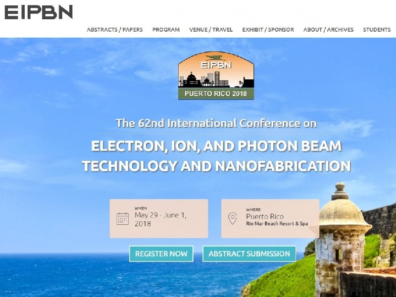
Sponsor at EIPBN Conference
Come to visit us !
We are proud to be a sponsor at the EIPBN conference this year!
Come to see our poster presenting our latest development on Delayering processes for failure analysis.
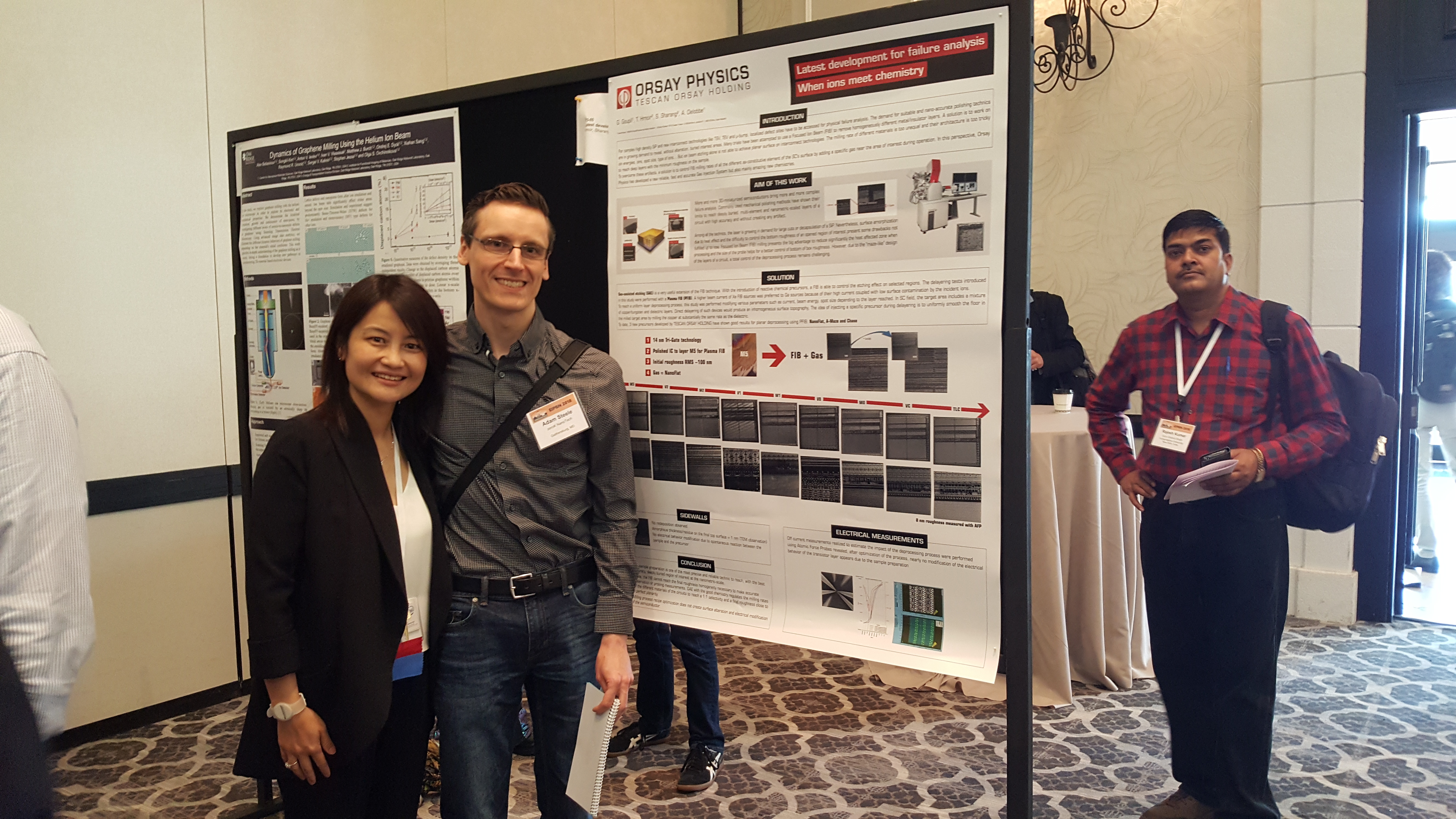
ICHORD : AU COEUR DE LA MATRICE CRISTALLINE
"ZOOM" sur le partenariat entre Orsay Physics, le laboratoire MATEIS et PULSALYS (SATT de l'Université de Lyon)
Orsay Physics, leader mondial de la technologie de faisceaux d’ions et d’électrons, fabrique des instruments de pointe (colonnes à faisceaux d’ions ou d’électrons localisés, microscopes électroniques à balayage, systèmes d’injection de gaz) pour l’analyse de matériaux à l’échelle nanométrique. Dans le but de maintenir l’excellence de ses produits et d’offrir de nouveaux outils à ses clients, Orsay Physics s’engage aux côtés de PULSALYS dans le développement d’une nouvelle technologie innovante de cartographie des orientations cristallines, mise au point par le chercheur Cyril Langlois au laboratoire MATEIS (INSA de Lyon).
L’aventure commence à Manchester en 2015, lors d’une conférence tenue par Cyril Langlois où il présente sa méthode innovante, iCHORD. Présente ce jour-là, Anne Delobbe, Directrice R&D d’Orsay Physics est immédiatement convaincue par son potentiel technologique. « La méthode iCHORD offrira une plus-value à nos machines », précise-t-elle. Elle contacte alors PULSALYS qui accompagne Cyril Langlois dans le transfert de sa technologie. La méthode vient d’être brevetée et recherche un industriel intéressé. Une opportunité pour Orsay Physics qui propose d’investir avec PULSALYS dans la maturation technico-économique du projet (150k€ au total). Le programme de co-maturation est lancé en novembre 2015, et se poursuit toujours. L’accord de co-développement a été assorti de la signature d’une option de licence exclusive avec Orsay Physics.
En quoi consiste la méthode iCHORD ? Laetitia Roux, Chef de Projet Instrumentation en charge du dossier, nous l’explique. « La méthode iCHORD (ion Channeling Orientation Determination) développée par Cyril permet de cartographier de manière précise l’orientation cristalline des grains (ou zones) composant les matériaux (métal, céramique…). L’orientation est directement liée aux propriétés de la matière ». Cette connaissance pointue de la structure cristalline peut être utilisée pour développer de nouveaux matériaux pour gagner en robustesse et en élasticité. Cette méthode trouve ses applications dans les marchés de la métallurgie, la mécanique et la céramique.
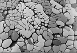
Images d’orientations cristallographiques
La méthode iCHORD améliore la technique de l’EBSD (Electron Back-Scattered Diffraction), actuellement utilisée. Ses atouts sont nombreux : un temps d’acquisition de l’image plus court avec une vitesse multipliée par 4, l’analyse de plus grandes zones d’échantillon, une meilleure résolution spatiale et un coût moindre car la méthode repose uniquement sur l’analyse d’images, grâce à un logiciel. Autre avantage, iCHORD peut être implémenté sur les appareils déjà présents au sein des laboratoires de recherche ou des laboratoires industriels.
Le programme de co-maturation avec Orsay Physics d’une durée de 18 mois a pour objectif de finaliser la preuve de concept en validant iCHORD sur divers échantillons « clients », et de l’amener à une solution industriellement viable. Cyril Langlois compte bien utiliser cette opportunité pour convaincre l’industriel de l’intérêt de sa méthode. « La preuve de concept laboratoire ne suffit pas, il faut convaincre l’industriel et pour cela la co-maturation est primordiale », conclut Cyril Langlois.
Nous avons échangé avec Cyril Langlois afin d'avoir son retour d'expérience sur ce co-développement
> Est-ce la première fois que vous faites du transfert de technologie ?
Oui et l’accompagnement apporté par la SATT est une vraie plus-value dans le développement de mon projet. PULSALYS m’aide à affiner la preuve de concept et c’est une étape importante pour convaincre l’industriel d’exploiter la technologie. Si l’on veut que notre invention serve à une application industrielle, la publication d’articles ne suffit pas, il faut intégrer un programme de maturation.
> De quel accompagnement bénéficiez-vous de la part de PULSALYS ?
La SATT s’est présentée comme l’acteur incontournable pour accompagner mon projet vers le marché. En effet, PULSALYS a très bien menée une des étapes importantes dans le programme de co-maturation qui est la négociation de l’option de licence avec Orsay Physics. Elle s’est également occupée de toute la propriété intellectuelle attachée au projet (base de données, brevet, logiciel), a financé une partie de la maturation et a apporté tous les moyens nécessaires (matériels, humains…).
> En quoi consiste la co-maturation avec Orsay Physics ?
La co-maturation a pour objectif d’aboutir à un produit répondant aux attentes réelles de l’industriel. Concrètement, la maturation permettra d’obtenir un prototype finalisé, de valider la technique sur plusieurs types de matériaux et de développer le logiciel d’analyse des données avec notre partenaire Axon Square. Le co-investissement entre PULSALYS et Orsay Physics s’élève à 150k€. L’investissement de PULSALYS a notamment permis d’embaucher un ingénieur maturation pour nous aider au développement de la méthode.
> Que vous apporte-t-elle ?
Le co-développement avec Orsay Physics apporte de nombreux avantages : une plus grande connaissance du marché, un investissement significatif dans le projet et un partage des risques.
> Pourquoi avez-vous choisi Orsay Physics pour votre transfert ?
Je dirai plutôt que c’est Orsay Physics qui m’a choisi (rires). La Directrice R&D Anne Delobbe était présente lors de ma conférence en Angleterre et suite à cela, elle a tout de suite perçu l’opportunité technologique que pourrait lui apporter mon projet. Orsay Physics fabrique des sources de faisceaux d’ions et ma méthode ne peut fonctionner sans. Il y a donc une complémentarité dans nos métiers et c’est ce qui a plu à Orsay Physics. D’autre part, c’est très agréable de travailler avec eux car ce sont des chercheurs et ingénieurs, qui comprennent parfaitement mes problématiques scientifiques, tout en apportant une logique business.
> Que ressentez-vous à l’idée que votre invention soit transférée sur le marché ?
Je suis très content que mon invention puisse servir à une application industrielle. Mon projet a grandi avec l’aide de PULSALYS et a bénéficié d’une plus grande visibilité.
> Quelles perspectives d’évolution pour votre projet ?
L’avantage de cette technologie est qu’elle peut s’appliquer à tous les domaines. Nous pourrions très bien imaginer une application en géologie par exemple. Nous sommes aussi en train de réfléchir à une technique pour modéliser les grains en 3D. Il y a de vrais potentiels avec la méthode iCHORD, tout reste à faire. C’est un challenge excitant.
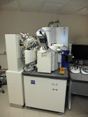
Cyril Langlois (premier plan) au laboratoire MATEIS et le
Microscope à balayage électronique pour l’analyse des grains cristallins
Pour découvrir la Newsletter de PULSALYS : http://p4l0.mj.am/nl2/p4l0/18qjx.html?m=ADwAH76Bcm4AAVfMf2cAAGbCEo8AAP__82AAGmvDAANvgABYxsDdIuztEAJ_TKSpp43vJnTvjQADSjg&b=77be9327&e=6ab8e69c&email=marie.planchet@orsayphysics.com
MICROSCOPY CHARATERIZATION OF ORGANIC-INORGANIC INTERFACES : HERE WE ARE !
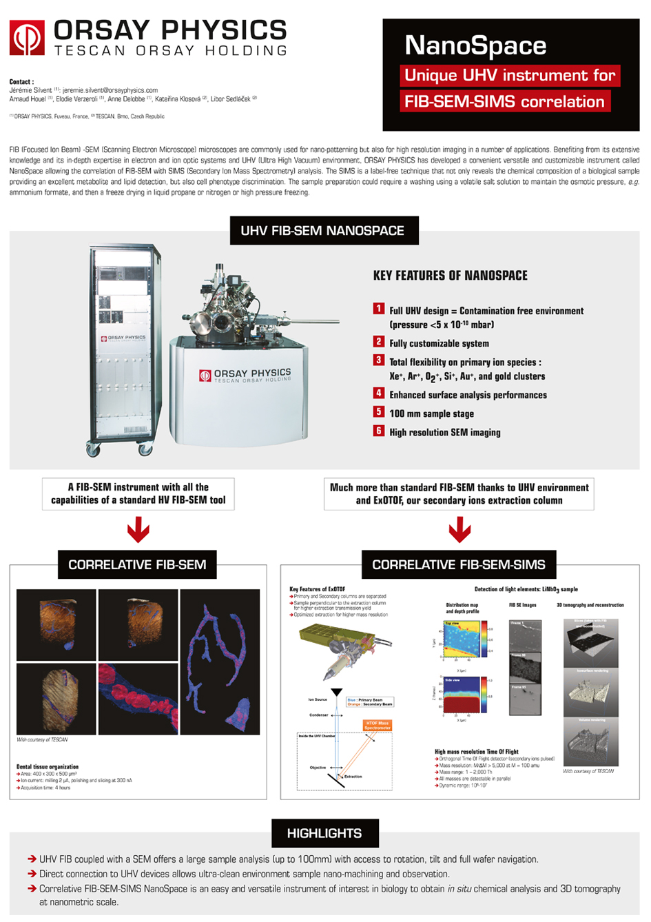
Currently, during these 2 days in London, ORSAY PHYSICS have a poster session for the life and materials science communities . We highlight our easy and versatile instrument, named NanoSpace, which enables biologists to obtain in situ chemical analysis and 3D tomography, at nanometric scale. Do not hesitate to have a look on our synthetic presentation of our correlative FIB-SEM-SIMS solution.
CALL FOR CANDIDATURES: THESIS (CIFRE grant) WITH ORSAY PHYSICS AND IM2NP
One of the bottlenecks in microelectronics industry is to determine the spatial distribution of materials constituting the devices of ultimate size. This requires chemical nano-analyses with large sensitivity and nanometric resolution. At such scales, the strain relaxation on the patterns edges induces inhomogeneous distribution of the elements which can become prohibitive for the use of ultra-small devices.
During this thesis, the target will be to provide a 3D mapping of benchmarked nano-systems (size, composition, strain and morphology fully known) in order to evaluate the specifications of SIMS nano-analysis and to optimize the instrument for this kind of applications.
The thesis (CIFRE grant) will be jointly realized in ORSAY PHYSICS (FUVEAU-13) and in IM2NP ( Marseille-13).
ORSAY PHYSICS has developed a new UHV equipment combining ultra-high resolution ion beam, scanning electron imaging, which will be adapted and coupled with a SIMS spectrometer for chemical nano-analyses. Furthermore, the NSE team of IM2NP is specialized in ultimate epitaxial deposition and nano-characterization of semiconductor nanostructures. The work will mainly consist of, on one hand, the elaboration of nanostructures of composition (morphology, size and shape controlled at the nanometer scale,) and on the other hand, the determination of their spatial chemical composition. The aim is to fit the SIMS nano-analyses specifications to the microelectronic requirements.
Thank you for sending your candidature to: isabelle.berbezier@im2np.fr
NEXT NanoSpace PROMOTION
We will participate in NanoSEA 2016 (http://www.nanosea2016.imm.cnr.it/) and in GDR Pulse Conference (http://www.im2np.fr/GDR_CNRS_Pulse/Marseille2016/index.html) promoting our new UHV FIB/SEM system (see NanoSpace in products section) whose specific configurations are fully adapted for nanostructures and nanomaterials research activities. For each event, you will be able to meet our sales engineer (contact@tescan-orsay.fr) at our stand or can listen our talk about NanoSpace’s key advantages and features.
A NEW APPLICATIONS ENGINEER JOB
ORSAY PHYSICS opens recruitment for an engineer to develop applications on SEM/TEM/STEM technologies coupled to FIB devices. To apply, write to: marie.planchet@orsayphysics.com
PIONEERS SCIENTIFIC APPLICATIONS
You are interested in scientific results obtained by renowned laboratories using ORSAY PHYSICS products : go to Applications section and discover their relevant researches. We will post regularly new Application Notes, hoping it will be a rich source of information for you, and an interesting promotion for scientific activities. Do not hesitate to contact us on these issues (contact@tescan-orsay.fr)
TWO UHV FIB-SEM NANOSPACE RECENTLY LAUNCHED
In May 2016, ORSAY PHYSICS installed its two first UHV FIB-SEM platforms (see NanoSpace in products section).
One in the LAAS (Laboratoire d’Analyse et d’Architecture des Systèmes, Toulouse) : clustered to a RIBER MBE UHV system via a connection chamber, NanoSpace will allow pioneers investigations on the next generation of III-V nanowires and quantum dots. It’s specific configuration: a plasma FIB (i-FIB) and e-CLIPSE Plus SEM column.
The second one in the IM2NP (Institut Matériaux, Microélectronique, Nanosciences de Provence, Marseille) is a standalone UHV device equipped with a Chroma ExB FIB and an e-CLIPSE Plus SEM column. IM2NP objective is to develop, with NanoSpace, new nanostructures and nanomaterials based on silicon components for optoelectronic applications.
It should be highlighted that Dr Isabelle BERBEZIER (IM2NP) and Dr Chantal FONTAINE (LAAS) coordinate a famous committee named GDR PULSE (Epitaxial ultimate process for semiconductors) which gathers French scientific actors on this issue.
(http://www.im2np.f/GDR_CNRS_Pulse/newsletter/Newsletter_GDR_Pulse4.html).
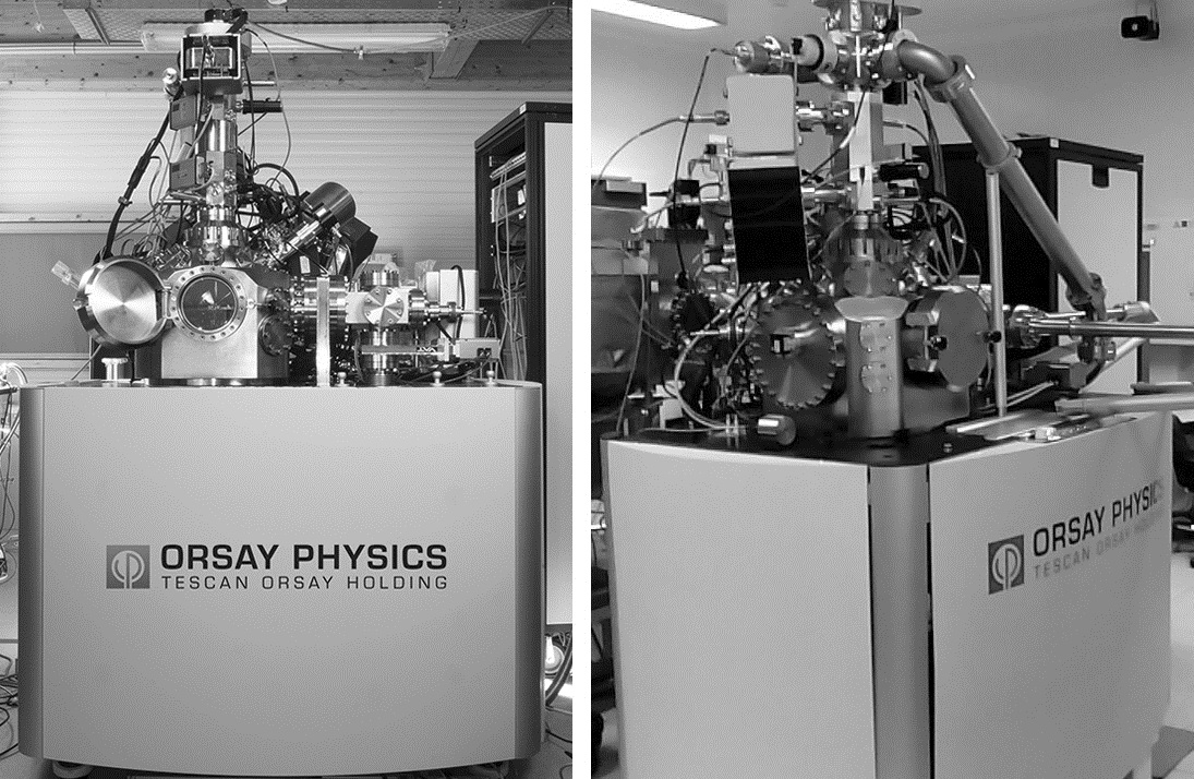
NEW FACILITIES IN FUVEAU (FRANCE)
Because of its continuous development, ORSAY PHYSICS started in 2016 the extension of its production building by doubling the surface to reach a total of 2 000 m2. In the same time, a new 400 m2 showroom is on progress to allow our group devices demonstration in France and applications development. By the end of 2016, 3 500 m2 of facilities will be on ORSAY PHYSICS area.
OUR BUSINESS
Takes just 5 minutes to discover ORSAY PHYSICS activities, especially how we develop a new and unique UHV dual beam platform, fully customizable and designed to give the possibility to connect it to a third UHV system. This technological advance was conducted in partnership with 2 French worldwide recognized academic laboratories (LAAS : Laboratoire d’Analyse et d’Architecture des Systèmes, Toulouse ; IM2NP : Institut Matériaux, Microélectronique, Nanosciences de Provence, Marseille) and the company RIBER, well-known in the Molecular Beam Epitaxy field. This collaborative research project was founded both by the French Government (AAP FUI 17) and local Authorities (Région Provence Alpes Côte d’Azur, Métropole Aix Marseille Provence).