Cobra ExB in the Andromede Project:
A rising generation of NAno Particle Ion Source (NAPIS) column
Andromede project (ANR-10-EQPX-23) is a new instrument for surface modification and analysis at the center of a multi-disciplinary team from Orsay University and CNRS led by S. Della Negra (director of research at IPN Orsay University). This equipment uses the impact of gold nanoparticles (Au400+4) in the keV to MeV range delivered by two ion sources in tandem, especially from the LMAIS (Liquid Metal Alloy Ion Source) FIB called NAPIS developed by Orsay Physics. This unique instrument will also study the fundamentals of nano-particle surface interactions.
Why such a project?
When a massive cluster impacts a surface at high velocity, a large volume of material is sputtered from the surface. The ionized portion of these material packs can be analyzed by mass spectrometry. In such conditions, the yield of molecular ions is significant, exceeding one molecular ion
per nano-particle impact and often surpassing a few ten molecular ions detected per impact. By coupling the mass spectrum obtained from a single projectile with the localization obtained from the microscope, imaging mass spectrometry can be performed on the event-by-event level. This has the distinct advantage of using coincidence methodology to study the co-localization of molecules at the nano-scale.
The goal of Andromede is to create a new imaging mass spectrometry instrument for the analysis of nano-fields and objects present on a surface with a spatial resolution of 20 nm. Moreover this instrument will give the opportunity to analyze the surface at atmospheric pressure and therefore the mass spectrometry analysis of native hydrated biological surfaces. This project is a very efficient alternative to the Secondary Ion Mass Spectrometry (SIMS). Molecular information (mass and structure composition) will be obtained from the impact of a nano-particle accelerated in the MeV range by a 1 to 4 MV NEC’s Van de Graaff accelerator.
Nano-particles sources
The two primary ion sources chosen for the project will be placed in tandem in the NEC’s accelerator terminal.
- An ECR will ionize species introduced through a gas inlet or evaporated/sublimated by an oven. It is possible to obtain multi-charged atomic ions as well as molecular ones such as fullerenes.
- A new LMAIS developed by Orsay Physics is capable of producing a range of metallic clusters (for gold: Aun+q: Au+, Au3+, Au5+, Au9+, Au100n+q. ). An all customized FIB was adapted to integrate this new source and to shape a perfect parallel beam at the column exit in order to be accelerated in the NEC accelerator. This FIB is a customized Orsay Physics Cobra ExB column called NAPIS.
NAPIS
The column is equipped with a LMAIS, two Einzel lenses (first condenser near the source and a focusing/decelerating lens after the mass aperture), two quadrupole deviators (one before the mass selection and one after), a Wien filter (for selecting the ion species according to their mass to charge (m/q) ratio), and a faraday cup.
NAPIS is able to produce gold clusters projectile up to Au400+4, from 20µA source current (high mass resolution mode) until 60µA for the Au nano-particle production. The gold source also produces AunGem+q or AunSim+q clusters due to the incorporation of about 4 wt% of Ge or Si.
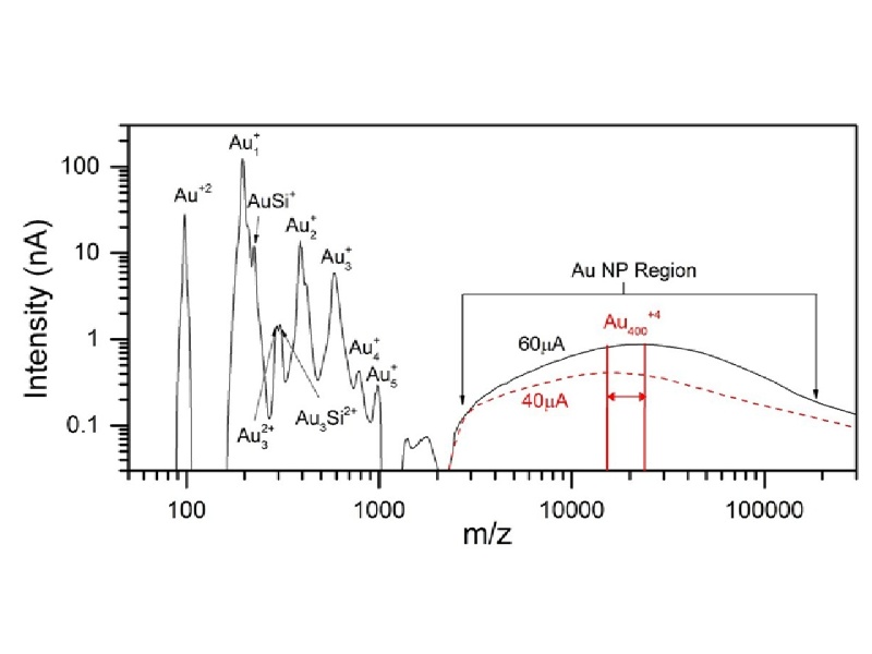
The mass spectrum of the ions produced by the gold germanium LMAIS can be found in the figure 6. The resolution achieved with the 20µm aperture is sufficient to resolve the five observable isotopes of germanium. The measured intensities are close to the isotopic ratio reported in the literature.
In nano-particle production mode, the extraction current is increased to 50-60µA, in such conditions a wide distribution of gold nano-particles are emitted from the source (see figure 7). The maximum distribution of emitted nano-particles is around n/q = 100 corresponding to an average of 400 gold atoms with a mean charge state of 4. In this condition, the source delivers more than 100 nA of Au+, 300 pA of Au5+ and 600-800 pA of Au400+4.
A key parameter in the production of gold nano-particles is the source current measured on the tip of the LMAIS. This current is directly related to the amount of ions produced from the source. It can be adjusted by varying the potential difference between the extraction electrode and the tip of the reservoir. As can be seen in the figure 7, the increased intensity of delivered nano-particles is accompanied by a shift in the mass distribution of the produced clusters. Thus, raising the extraction potential it is possible to increase the intensity of nano-particles as well as their average mass. Therefore, optimum conditions are achieved for the production of the selected nano-particle, Au400+4, with an extraction current of 50-60 µA.
IGLEX
The Andromede Project is currently under validation tests and will be shortly installed in a new facility of the University Paris Sud Orsay called IGLEX. In this facility two EQUIPEX projects will be set in one place (Andromede and ThomX). This new multi-disciplinary facility will boost collaborations between physicists, chemists, biologists and medical researchers.
References
- http://ipnwww.in2p3.fr/ANDROMEDE, 384
- M.J. Eller and al., Nuclear Instruments and Methods in Physics Research B 365 (2015) 367-370
- S. Della-Negra, Andromede project, from dream to reality, SIMSXX 2015, poster
- S. Della-Negra, Andromede unique tool to produce and analyze nano-objects,
Innovation review CNRS, April 2016, N°93, p38-40
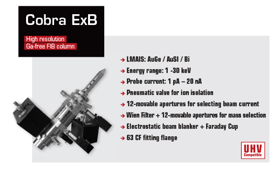
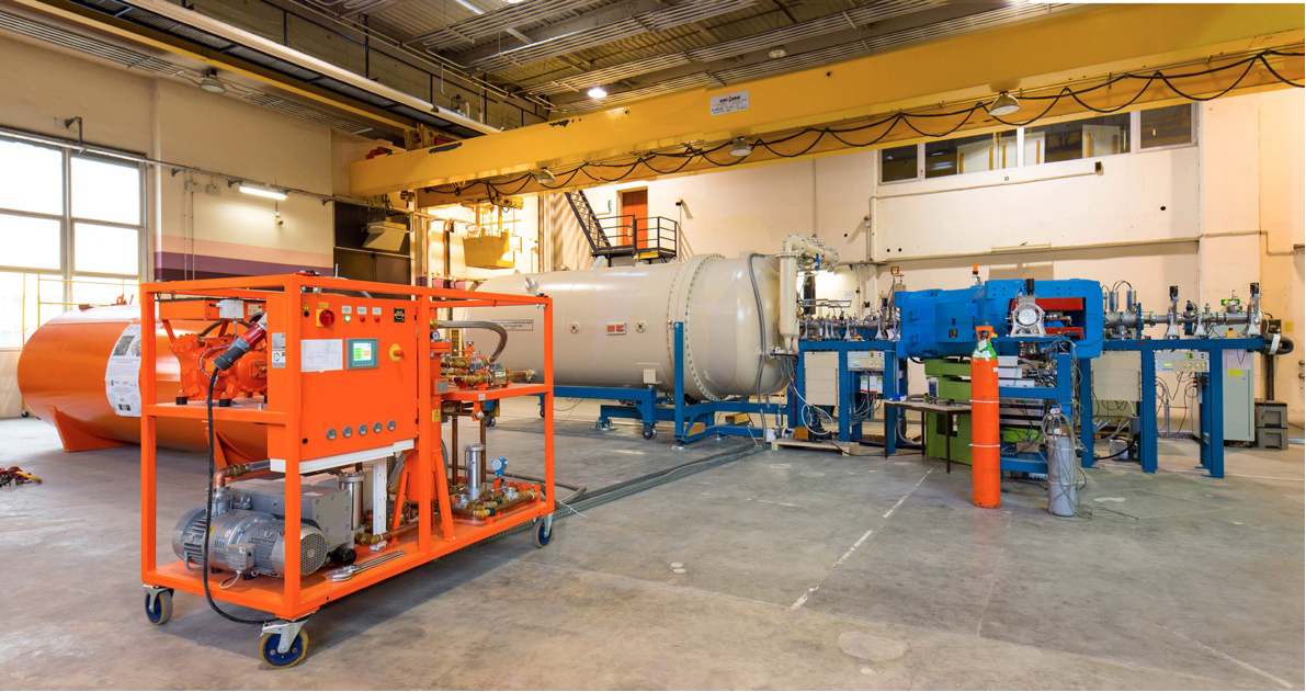
Figure 1. Andromede accelerator facility
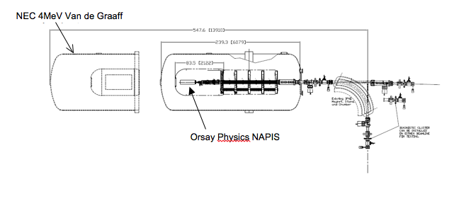
Figure 2. Andromede project view from above
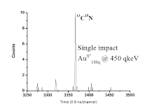
Figure 2. Time of flight mass spectrum of the emitted negative
ions from glycine target under a SINGLE impact of Au100nq+ at 450 qkeV
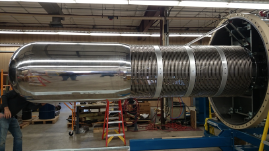
Figure 3. Inside the NEC Pelletron 4MeV accelerator
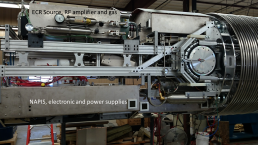
Figure 4. NAPIS and ECR ion sources installed on NEC
accelerator terminal
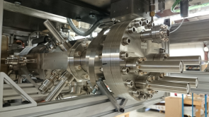
Figure 5. NAPIS FIB integrated in NEC terminal
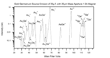
Figure 6. Mass spectrum of ions produced from NAPIS AuGe eutectic
in high mass resolution mode with an extraction current of 20µA
Notice the germanium isotopes are all separated.
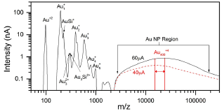
Figure 7. Mass spectrum of the delivered Aun+q projectiles from
the LMAIS eutectic in nano-particle production mode.
The region of Au400+4 is highlighted in red.