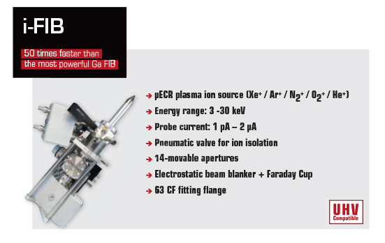
Xe plasma FIB (i-FIB) Delayering technology
using water as Gas-Assisting Etching (GAE) enhancer
Fast milling rates and high quality artifact-free surfaces are two essential and desired elements when preparing cross-sections in samples for the purposes of failure analysis. Gas introduction using a 5-line GIS coupled with i-FIB Orsay physics’ plasma ion source column reduces dramatically the time for cross-sectioning and planar etching from tens of hours or even days to a matter of hours.
The burgeoning generation of electronic data and the growing need for fast processing is driving the development of unique architectures in microelectronic devices. High device performance, along with low energy consumption, decreasing device area and optimal production costs are the four basic tenets of operation in the microelectronics industry [1]. These rules have led to ever-increasing area density of the basic elements in electronic devices and consequently to element’s shrinkage to the nanometer scale. This has brought new challenges for production technologies as well as for failure analysis of such devices.
State-of-the-art standard electronic devices are based on 22 nm and 14 nm node technology and the next generation of 10 nm and 7 nm nodes are already under development [1]. These technologies call for unique instruments and workflows for the identification and excavation of nanometer-sized faults buried under the device surface. Mechanical polishing as a standard tool in the failure analysis process does not meet the very strict requirements of these state-of-the-art nodes. The thickness of metal interconnects and dielectric separating layers just above the transistors has shrunk to less than 100 nm. Therefore it is a challenge to stop the polishing process in a particular layer with the expected quality, accuracy and repeatability. Moreover, mechanical polishing, mostly accompanied by surface artefacts like material chipping-off and site-specific fault excavation, is usually impossible. Focused Ion Beam (FIB) technology using has proven to overcome these restrictions. It offers the possibility to target a failure with nanometer accuracy in depth as well as in the lateral direction. Therefore cross-sectioning, site-specific layer-by-layer excavation (also known as delayering) and direct extraction of a Transmission Electron Microscopy (TEM) lamella containing the particular fault of interest have become standard methods in failure analysis.
This note presents delayering of a processor based on 14 nm node technology [2]. The delayering is performed with a Xe plasma focused ion beam (i-FIB column). Beam currents of Xe i-FIB up to 2 µA have extended the dimensions of the analyzed volume of interest to several hundred micrometers in general [3,4], while simultaneously enabling homogeneous delayering with nanometer accuracy. Xe source is advantageous also because interaction of inert Xe atoms with the material surface does not significantly alter either the properties or the reactivity of the material. Thus the ability of Xe to induce surface contamination is negligible.
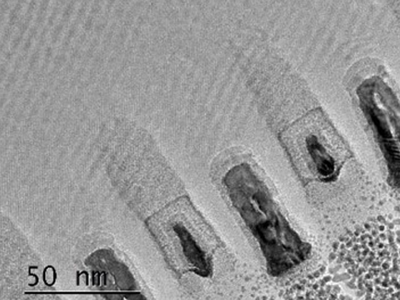
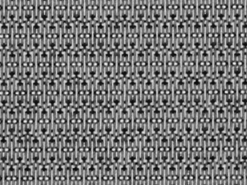
Processor architecture is based on alternating metal and dielectric layers (Fig. 1). These layers have different sputtering rates when FIB delayering is applied. Uneven sputtering can be substantially controlled by chemical means. In our experiments, water vapor was delivered directly to the point of patterning via a 5-line GIS (Gas Injection System developed by Orsay Physics) in order to equalize sputtering of metal interconnects and insulators. The result of processor delayering down to the first metal layer, just above the transistors is shown in Fig. 2. The damage-free surface of the transistor contact layer is ready for electrical probing.
Nanometer-sized elements in state-of-the-art electronics have posed a challenge also for imaging technologies. Clear observation of the very thin individual layers means suppressing the acceleration voltage of primary electrons to the sub-1 kV range, ideally to 500 V. At higher energies, the electron signals from different layers would intermix as they are generated in a volume comparable to the thickness of those layers. However, sub-nm resolution at low electron energies is a necessary condition due to the size of the observed features. High resolution pictures captured at 500 V are shown in Fig. 2. Low-kV imaging has verified highly homogeneous delayering of the processor as can be seen by the absence of large contrast changes in the delayered region.
References
[1] http://www.itrs2.net/
[2] http://www.intel.com/content/www/us/en/silicon-innovations/intel-14nm-technology.html
[3] T Hrnčíř et al., 38th ISTFA Conf. Proc. (2012), p. 26.
[4] A Delobbe et al., Microsc. and Microanal. 20 (2014), 298.
[5] T Hrnčíř et al., 41th ISTFA Conf. Proc. (2015), p. 60.


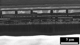
Figure 1. Processor (14 nm node) after mechanical
polishing and Xe i-FIB cross-sectioning.
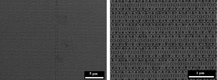
Figure 2. Top view of the transistor contact layer in a commercial
Processor (14 nm node) after the delayering process obtained with
a TESCAN XEIA3 FIB-SEM system (i-FIB column).
A global overview (left) and close-up micrographs (right) are taken
with a SE detector at 500 V using beam deceleration mode.