Curtaining-Free Top-Down TEM Lamella Preparation
from a Cutting Edge Integrated Circuit using a
Rocking-Stage and water as Gas-Assisting Etching
(GAE) enhancer
Diminution of FIB polishing artifacts such as curtaining or delayered surface roughness is the key for the comprehension of the failures at the nanoscale dimension. The association of a specially designed Rocking stage, FIB columns and a 5-line GIS gives the possibility to reach smooth surfaces or curtaining-free cross sections suitable for advanced analysis such as TEM lamella preparation or semiconductor failure analysis.
Semiconductor industry continues to shrink sizes of the electronic devices. Currently commercial state-of-the-art technology node for integrated circuits is 14 nm, while 10 and 7 nm technology nodes are in the development stage [1]. Those integrated circuits are based on multigate transistors, where source-drain channel surrounded by a 3D gate. Failure analysis process of such integrated circuits typically involves inspection of TEM lamellae prepared by FIB-SEM machines from a single transistor layer.
One difficulty in preparation of such TEM lamellae is different ion milling rates of materials of the integrated circuits. In case of conventional top-down FIB polishing, this causes unwanted curtaining artefacts resulted mainly from the metal contacts above the transistor layer. One way to eliminate curtaining (see figure 1) is so called backside (or inverted) polishing technique which involves lamella extraction, flipping and polishing by FIB through the silicon layer [2]. However, this technique is too much time consuming for a daily semiconductor industry process.
A new technique of curtaining-free lamella preparation was found in the TESCAN ORSAY group. This technique allows for normal top-down FIB polishing through upper metal contacts while curtaining artefacts are eliminated by changing the incident angle of ion milling by rocking of the sample on a special TESCAN rocking stage.
In order to demonstrate this technique, we took the latest commercially available processor based on 14 nm technology node (Intel Pentium G4400) [3]. The processor wafer was decapsulated and mechanically polished to remove the top metal contacts. Further delayering (homogeneous layer etching) was performed by means of a specially developed technique of water-assisted plasma FIB etching (i-FIB column). The later technique allows uniform damage-free delayering down to the first metal layer which is just above the transistor layer (Fig. 2a). The delayered sample was transferred to a TESCAN GAIA3 FIB-SEM instrument which was equipped with a Ga FIB column (Cobra), a SEM column with immersion optics and a Rocking stage [4].
Initial steps of a lamella preparation involved a standard routine of platinum protection layer deposition using a 5-lines GIS developed by Orsay Physics, FIB trench milling, undercut and lamella transfer by a nanomanipulator to a TEM half-grid for the final thinning.
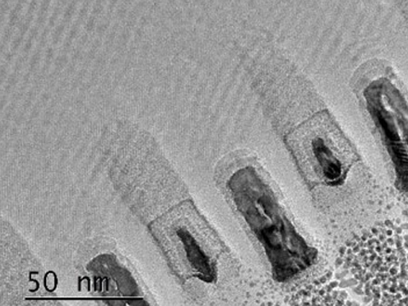
Lamella thinning was performed by Ga Cobra FIB at 30 kV till reaching the lamella thickness of 150 nm. The last step of thinning down to the thickness of less than 20 nm was performed by 5 and 2 kV FIB polishing (see perpendicular “fin-cut” for illustration on Fig. 2b). The final lamella was prepared just in the middle of a single fin (so called “gate-cut”). Moreover during the last steps of FIB thinning the lamella was milled from two directions on the Rocking stage (Fig. 3a). Thus due to continuous change of Ga beam incident angle (±15º) curtaining artefacts were eliminated.
Finally, the prepared lamella was transferred to a TEM microscope for observation. The observation demonstrated that even though the lamella was polished by Ga FIB by top-down technique through upper metal contacts it does not show evidence of any significant curtaining artefacts (Fig. 3b). This result proved the potential of the technique of top-down lamella thinning on a TESCAN Rocking stage.
References:
[1] http://www.itrs2.net/
[2] O Ugurlu, M Strauss, G Dutrow, J Blackwood, B Routh, C Senowitz, P Plachinda, and R Alvis, Proc. of SPIE 8681 (2013), p. 868107.
[3] http://www.intel.com/content/www/us/en/silicon-innovations/intel-14nm-technology.html
[4] T Hrnčíř, J Dluhoš, L Hladík, E Moyal, J Teshima, and J Kopeček, 40th ISTFA Conf. Proc. (2014), p. 136.
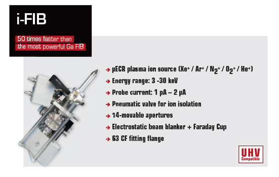

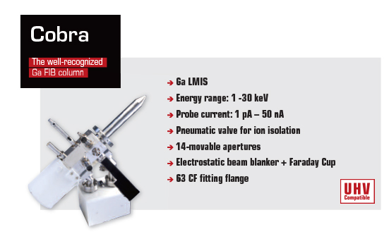
Figure 1. Curtaining effect observed on a cross section
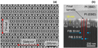
Figure 2. (a) Top view image of the first metal layer after delayering
by water-assisted Xe Plasma FIB (i-FIB on XEIA3) etching. (b) “Fin-cut”
of the chip illustrating the place and procedure of further lamella thinning.
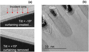
Figure 3. (a)Thinning the lamella on a Rocking stage: altering
the ion incident angle by ±15º eliminates curtaining. (b) TEM image
of the lamella prepared in the middle of a single fin (“gate-cut”)
shows no significant evidence of curtaining artefacts.