Ultimate nanopatterning of Si substrate
with Cobra ExB mass-filtered FIB column
With the increasing demand of high reproducibility, speed and resolution of pattern process fabrication in the nano- and microelectronics, ultimate nanopatterning must be achieved. Cobra ExB FIB technology is a Liquid Metal Alloy Ion source (LMAIS) which offers unique capabilities to create patterns with extreme size and shapes designed on demand due to the maskless process while using non-polluting ion source.
Led by Dr. I. Berbezier, team leader at IM2NP-CNRS Aix-Marseille University in France, the French academic team has studied the influence of the major FIB operating parameters (ion chemical species, beam current, lens voltage and ion dose) on the ultimate nanopatterning resolution. The main advantage of LMAIS FIB is the flexibility of its direct local one step patterning as compared to the costly and complex electron beam lithography (EBL) technique that requires numerous steps. They propose a two-step process based on first FIB milling of a SiO2 sacrificial layer and second SiO2 chemical etching for the fabrication of nanopatterns with the ultimate size/density and whatever shape. Their experiments are made on a TESCAN LYRA1 equipped with Cobra ExB developed by Orsay Physics. In a LMAIS, the ion beam is constituted of the elements of the alloy which can be separated by a Wien filter according to their mass to charge ratio for the selection of one specific specie.
Milling conditions
One preliminary level is to determine the minimum FIB dose (= ion current x milling time) to produce milling (= erosion/implantation ratio larger than unity). When increasing the ion current, the morphology of the patterns switched from mounds (implantation see figure 1a) to holes (milling see figure 1b) for doses of 0.05x10¹⁴ and 4.06x10¹⁵ ions/cm²/s respectively. For the next experiments, LMAIS FIB is in the milling condition.
High resolution nanopatterns process
Dr. I. Berbezier’s team developed a two-step process to produce high resolution patterns with Cobra ExB. The optimized experimental conditions are a very low probe current (1-6 pA) and low dose (milling time 5-30 ms). The Ga+ primary ions are used and the column is perfectly aligned with the focused beam at the sample surface. The patterning process (figure 2) involves first Cobra ExB FIB of an ultra-thin SiO2 layer and second the chemical etching of the SiO2 layer. In such conditions, ultimate size and density of nanopatterns can be achieved.
An example of the AFM images of SiO2/Si (100) nanopatterned in optimized conditions is given in figure 3a. The mean pattern size measured is 35 nm. TEM cross-section observations of LMAIS-FIB pits performed in ultra-thin oxide show a pit diameter of 15 nm regularly spaced every 150 nm (Figure 3b). One can see on this image that the controllable pit depth h = 6 nm reaches the Si substrate and penetrates in the substrate with a reproducible depth penetration of 1 nm.
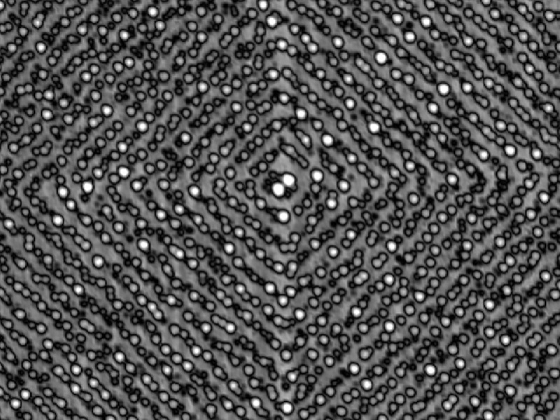
The flexibility of the Cobra ExB pattern shape is evidenced in figure 4a where Vasarely painting is reproduced by ion milling. Also circles extending over 400 × 400 μm2 are produced (figure 4b).
Then the same nanopatterning is performed but the distance between the patterns to 24 nm is reduced. In a second step the sacrificial ultra-thin SiO2 layer is removed by chemical etching. The nanopatterns obtained (figure 5) exhibit a pitch of 24 nm and a lateral size 15 nm. The shape of the patterns can be tuned and varied ad libitum using a script of the design to be drawn on TESCAN LYRA1 software.
Thus, these results show that both the size and the position of each pattern can be controlled at the nanometer scale by varying different LMAIS FIB milling parameters. Moreover Cobra ExB nanopatterning process can be used for efficient Si wafer nanostructuring. The two-step process described in this note allows the fabrication of patterns with ultimate resolution of 15nm (~4x10¹¹ patterns/cm²) and whatever shape spaced of 24 nm.
References:
- A. Benkouider, et al., Ultimate nanopatterning of Si substrate using filtered liquid metal alloy ion source-focused ion beam, Thin Solid Films (2013).
- I. Carmen Marcus, et al., In-Plane Epitaxial Growth of Self-Assembled Ge Nanowires on Si Substrates Patterned by a Focused Ion Beam, Cryst. Growth Des. 11 (2011) 3190.
- M. Aoussa, et al., Design of free patterns of nanocrystals with ad hoc features via templated dewetting, Appl. Phys. Lett. 101 (2012) 013117.
- http://www.im2np.fr/recherche/equipes/si-ge.html
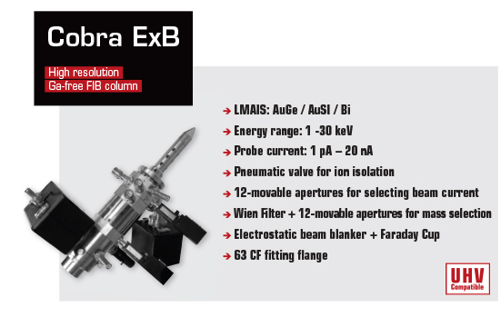

Figure 1. AFM images of the patterns obtained under different Cobra ExB FIB irradiation conditions
(a) Implantation: 0.05x10¹⁴ ions/cm²/s (b) Milling: 4.06x10¹⁵ ions/cm²/s
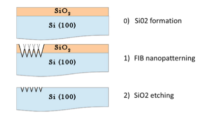
Figure 2. Schematic representation of the optimization two-step process
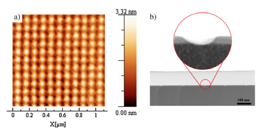
Figure 3. (a) AFM and (b) TEM images of the ultimate nanopatterning produced by Cobra ExB using 1 pA Ga+
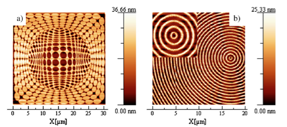
Figure 4. AFM images of the patterns obtained under the optimization process
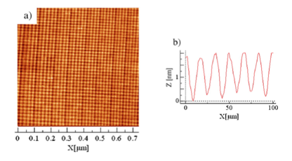
Figure 5. (a) AFM image of the ultimate nanopatterning (b) The mean pitch and pattern diameter measured
on the line profile are 24 nm and 15 nm respectively