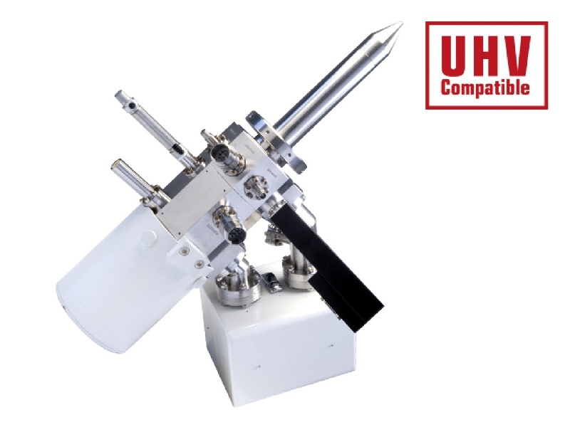
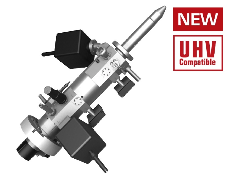
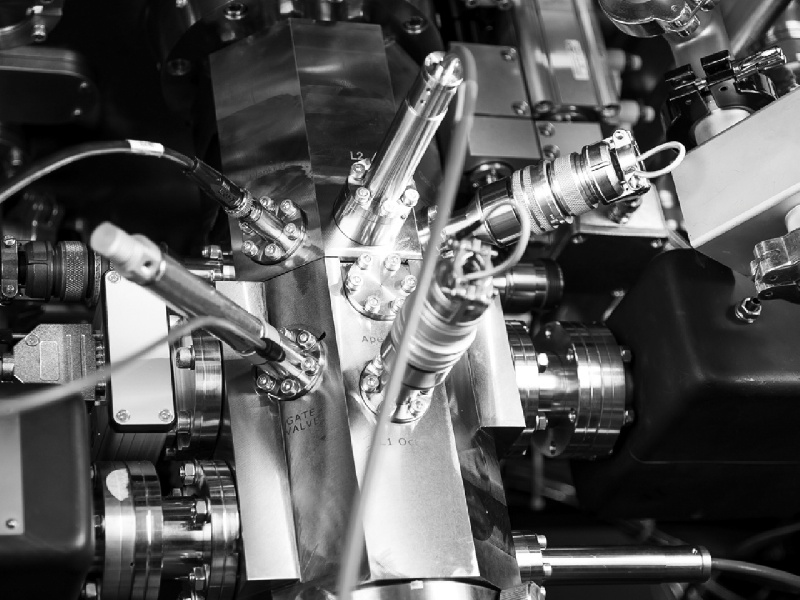
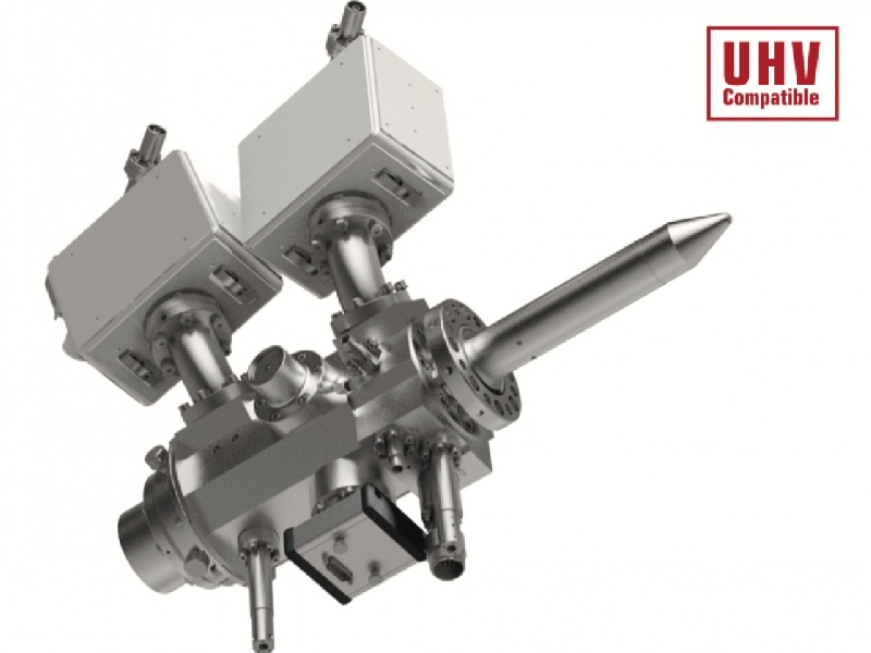
World leader in customized focused ion and electron beam technology

cheap replicas rolex daytona 116505 supplies a helpful details regarding observe experts and also lovers. the best knockoff rolex datejust m279384rbr 0019 rolex calibre 2671 mingzhu engine ladies white dial in the world integrate with the fantastic watchmaking connotation.

FIB


DeepFIB

Unleash the power: Redefying limits of the gallium focused beam

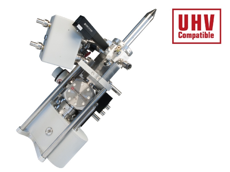
DeepFIB is our very last Ga FIB column released. DeepFIB extends the panel of applications thanks to both an optimized design for low energy work and a sharply focused beam even for high currents.

DeepFIB column allows to reach the smallest resolution at high acceleration voltage (< 2.5nm) and at low energy (<400 nm @500 eV) and to keep an ultra-fine resolution in a wide range of possible currents. The high current mode increased up to135 nA enables a faster milling and a huge time saving keeping the sharpest beam.

DeepFIB is easily adaptable on any vacuum chamber as it is also available in a UHV configuration and so bakeable up to 120°C. DeepFIB has a large field of view (1000 μm x 1000 μm) allowing to locate easily the regions of interest.

  Key Features

  Source

  LMIS (Liquid Metal Ion Source)

  Ion Species

  Ga+

  Energy Range

  500 eV - 35 keV

  Probe Current 

   <0.3 pA – 135 nA

  Working  Distance

  12 mm

  Ultimate resolution - 35 keV

  <2.5nm

  Ultimate resolution - 1 keV

  <115 nm

  Ultimate resolution - 500 eV

  <400 nm


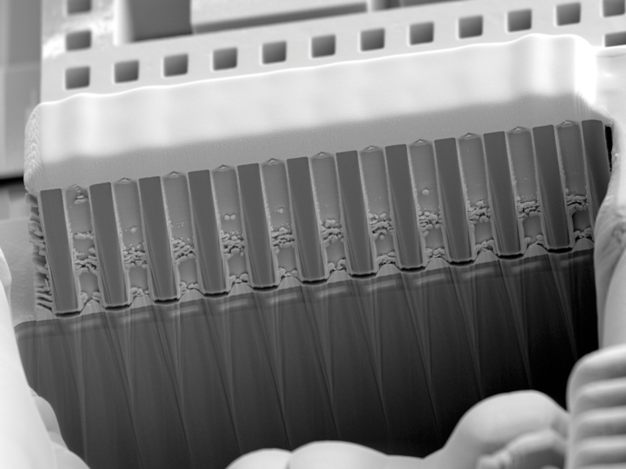
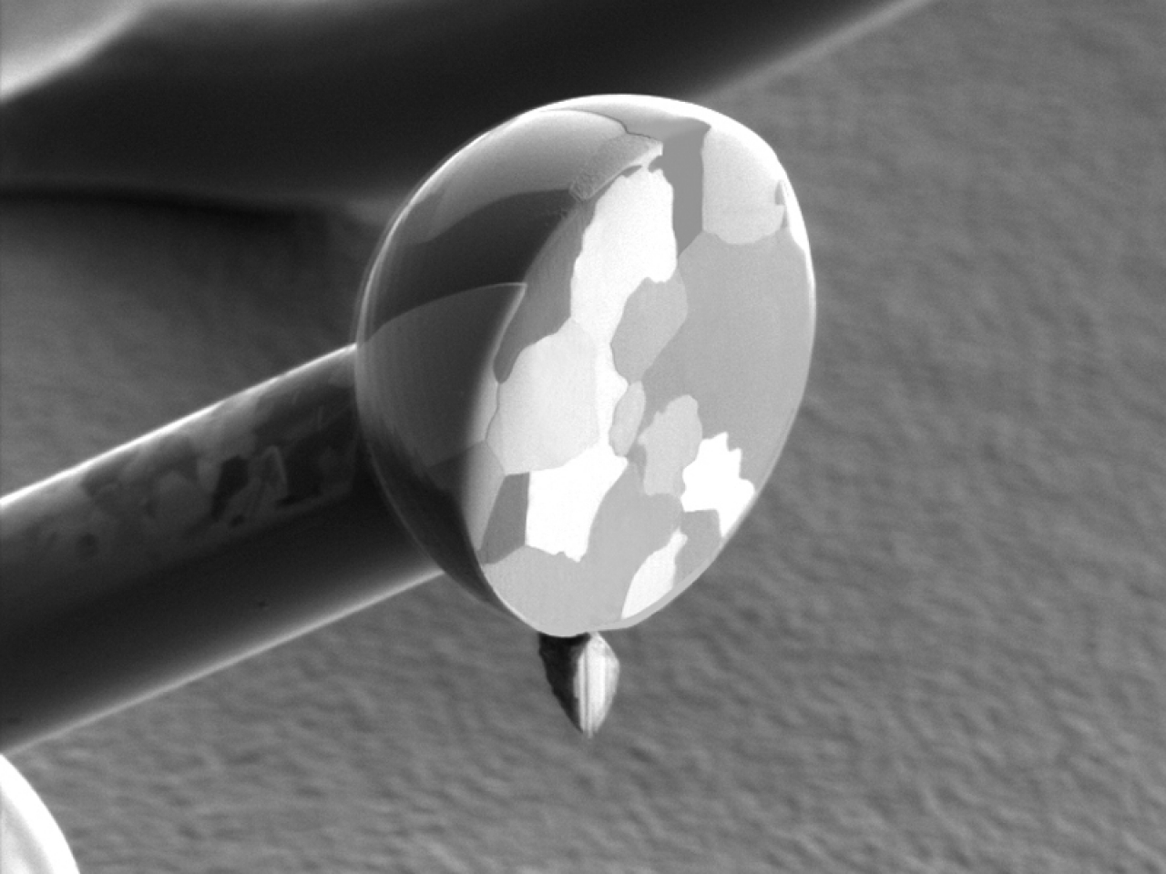
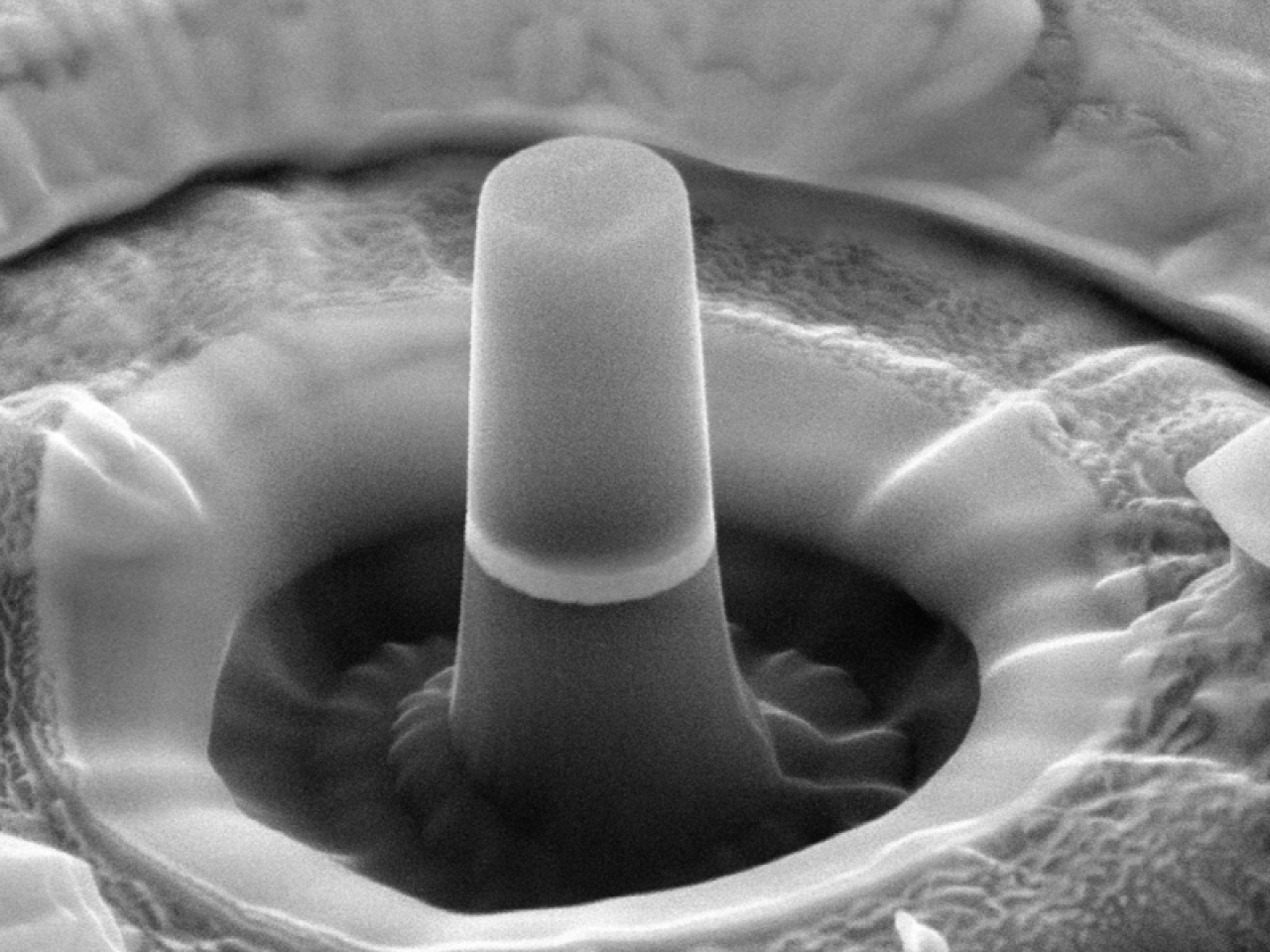
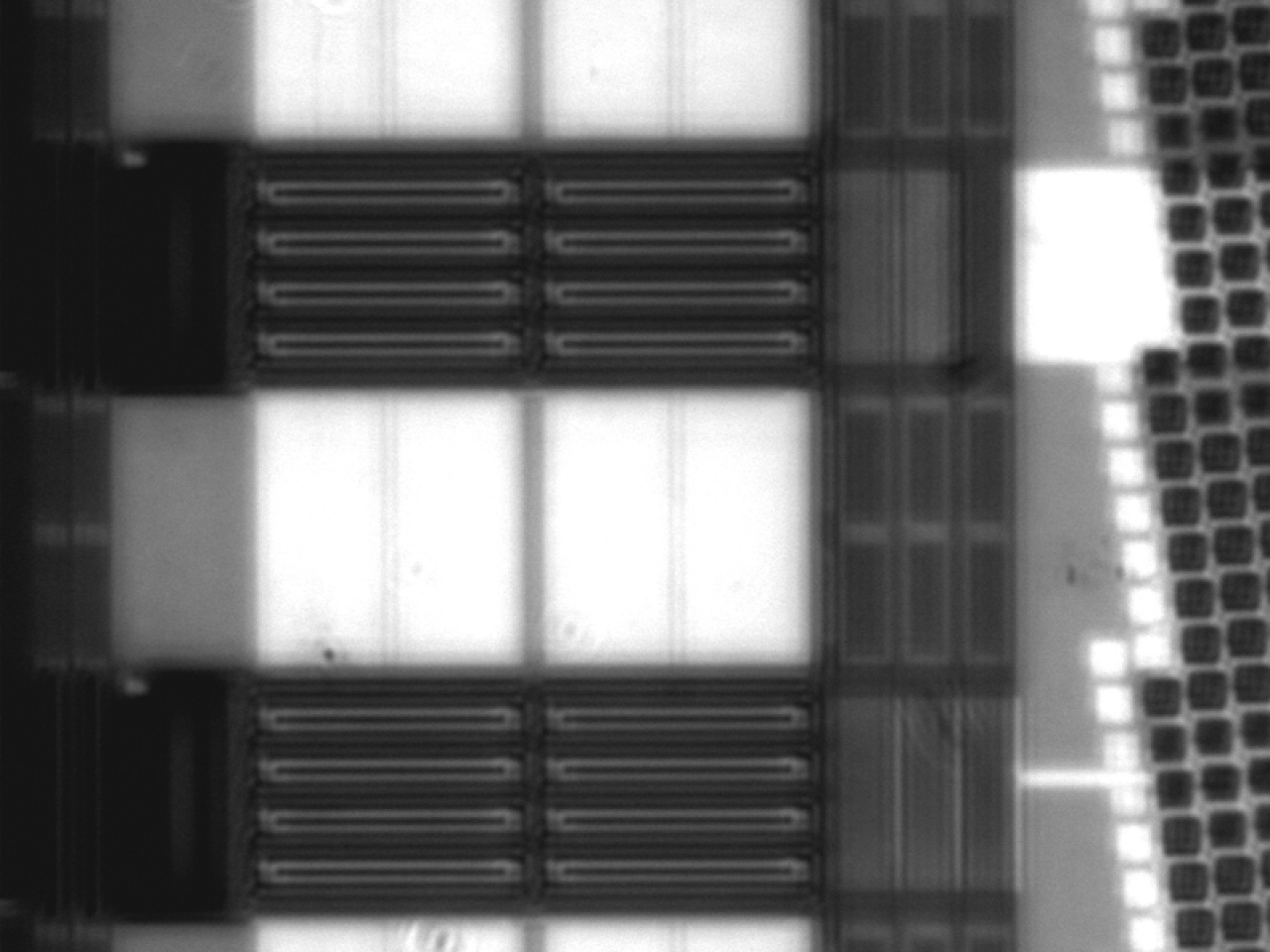
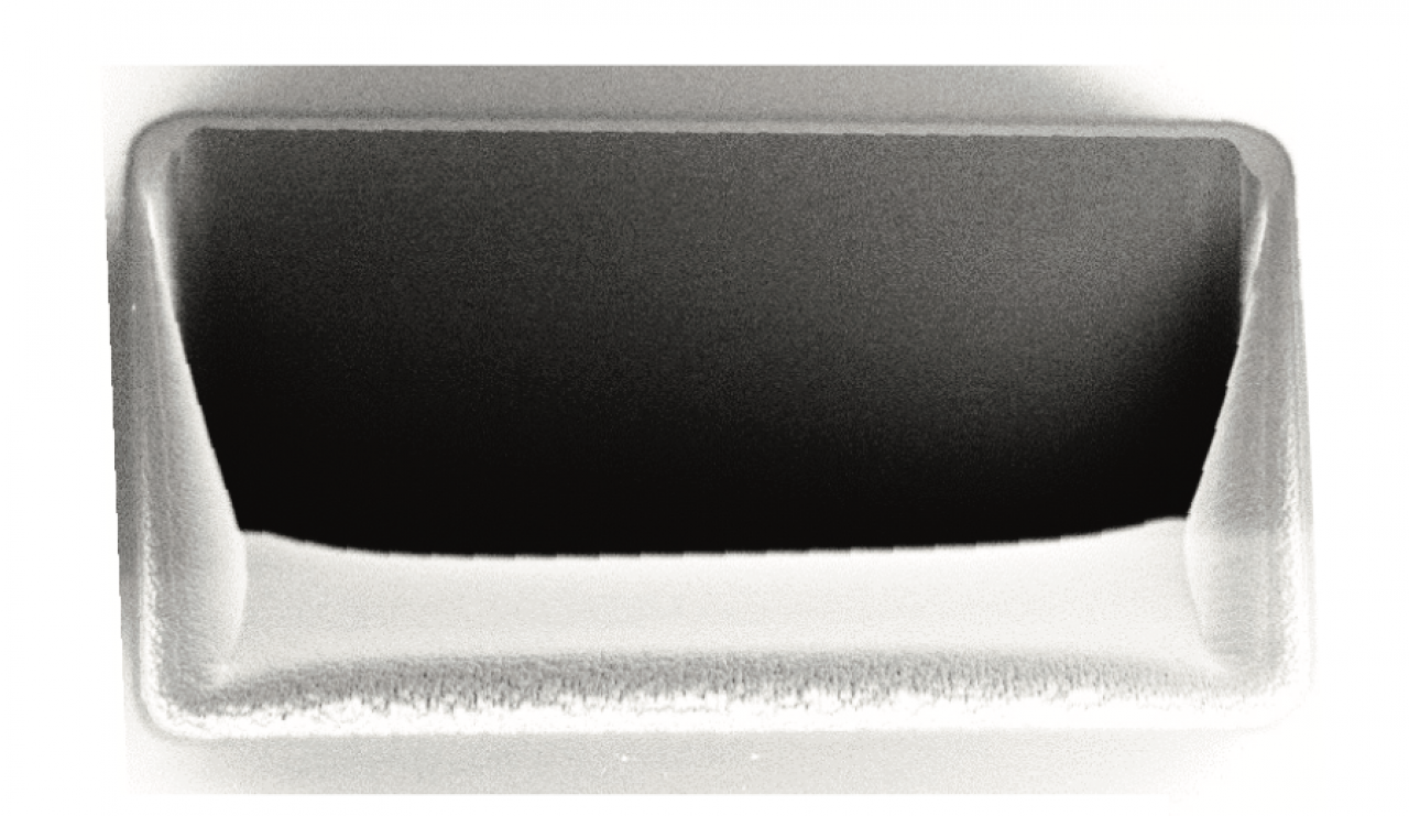
  • High-resolution perfomance at low energy allows to perfom a TEM lamella final polishing step at 1 keV

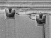
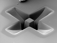
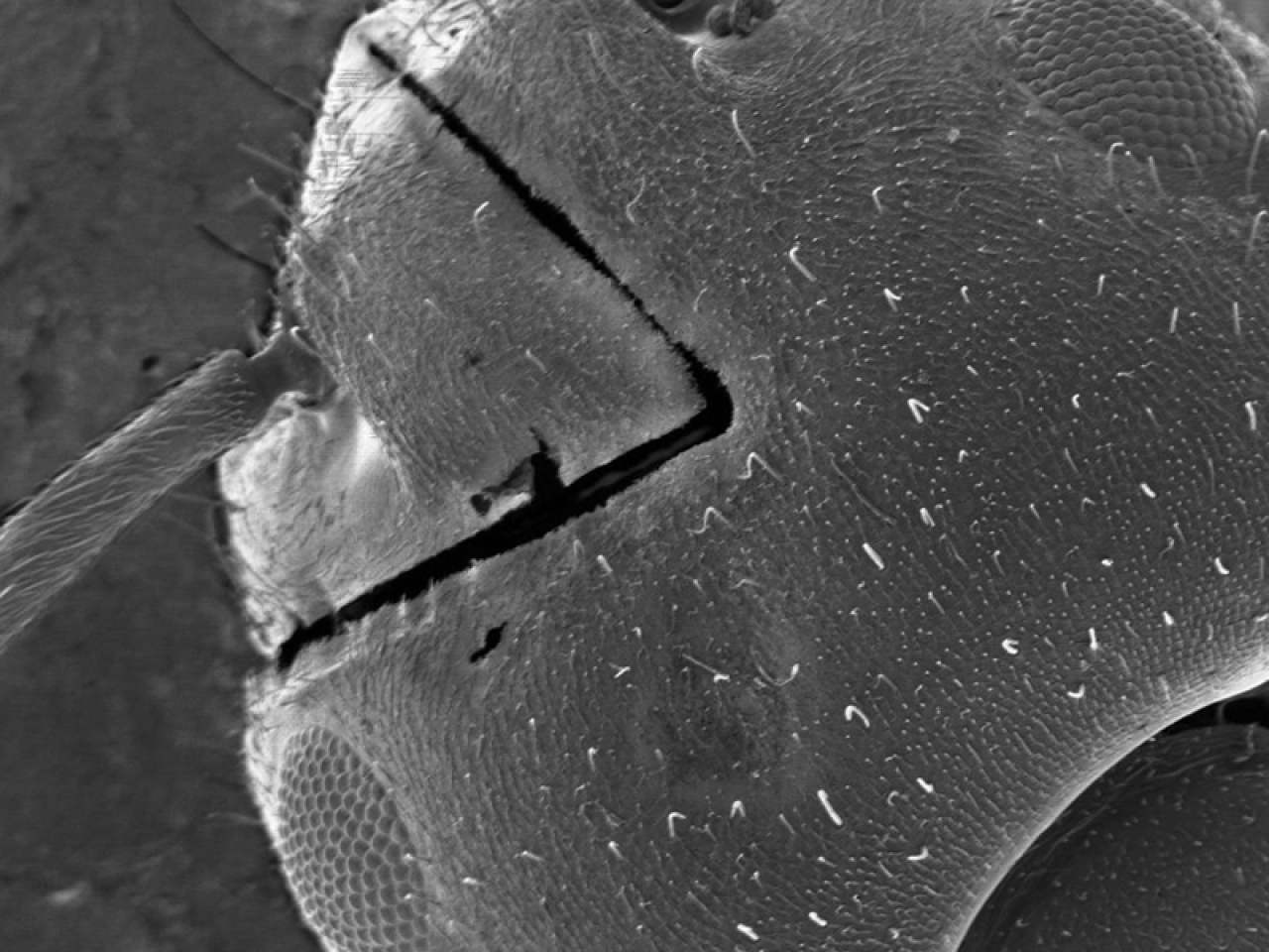
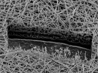
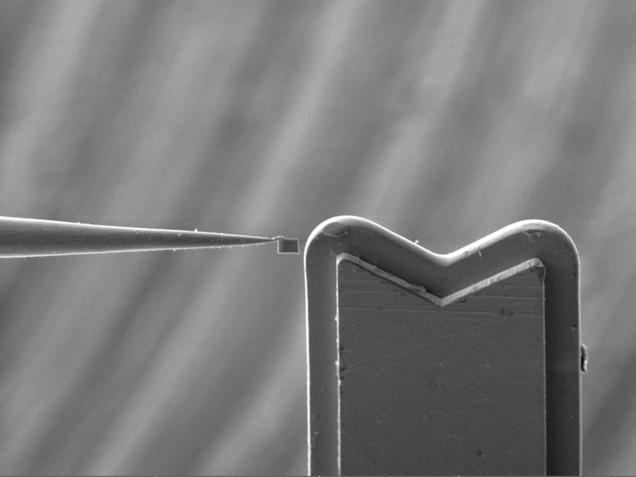
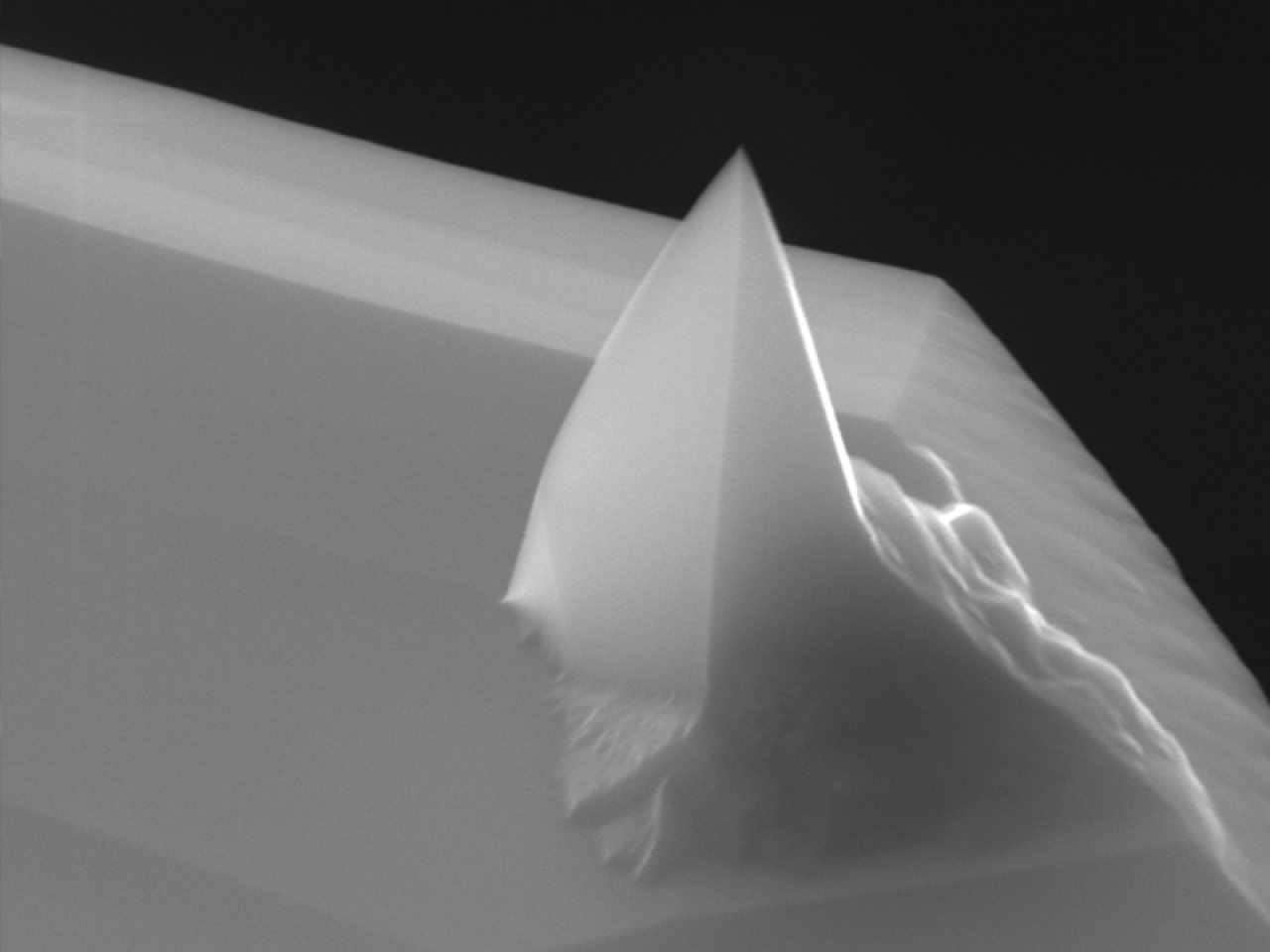
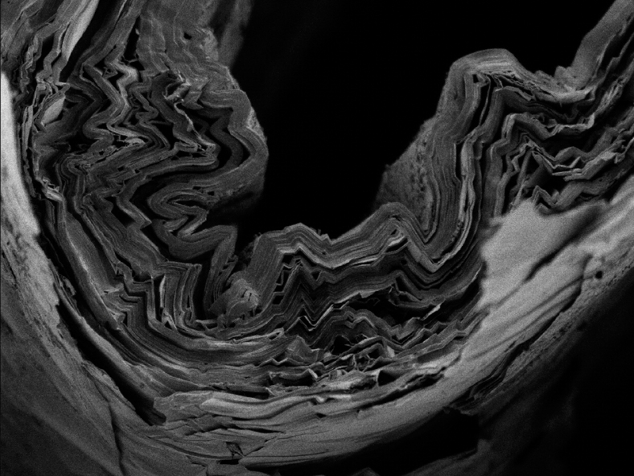
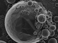
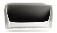
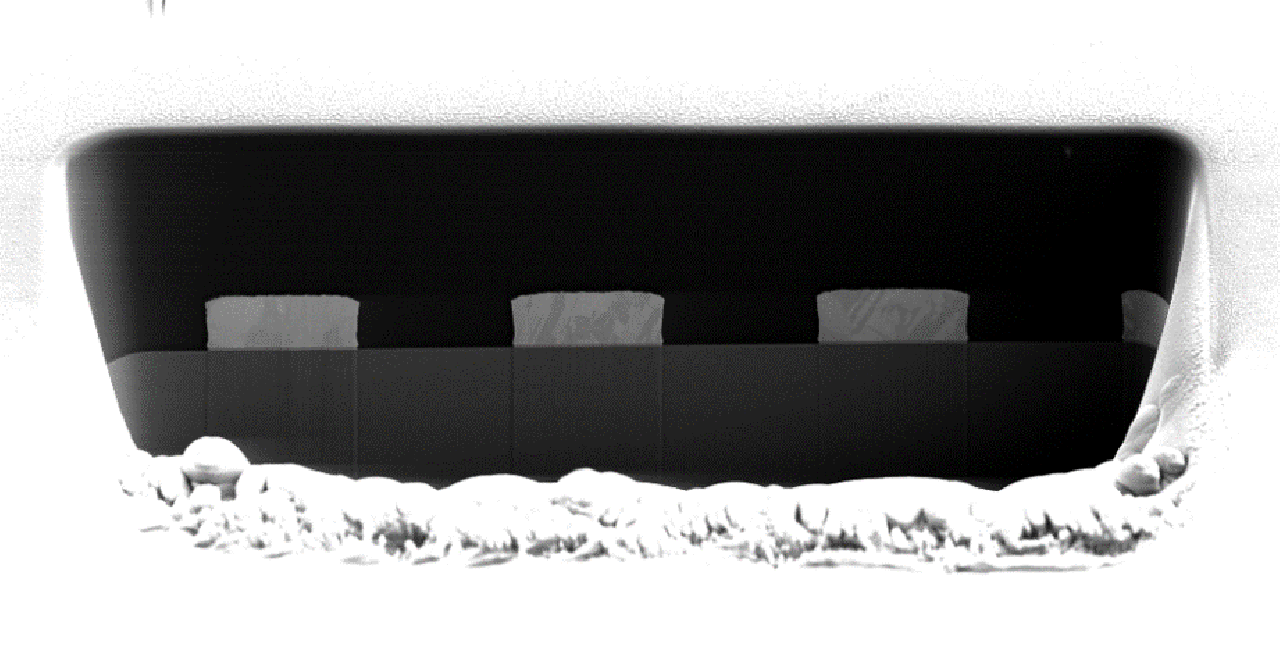
  • A high-quality cross-section of Si (80x50μm) obtained @135 nA in 30 min

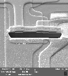
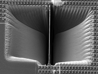
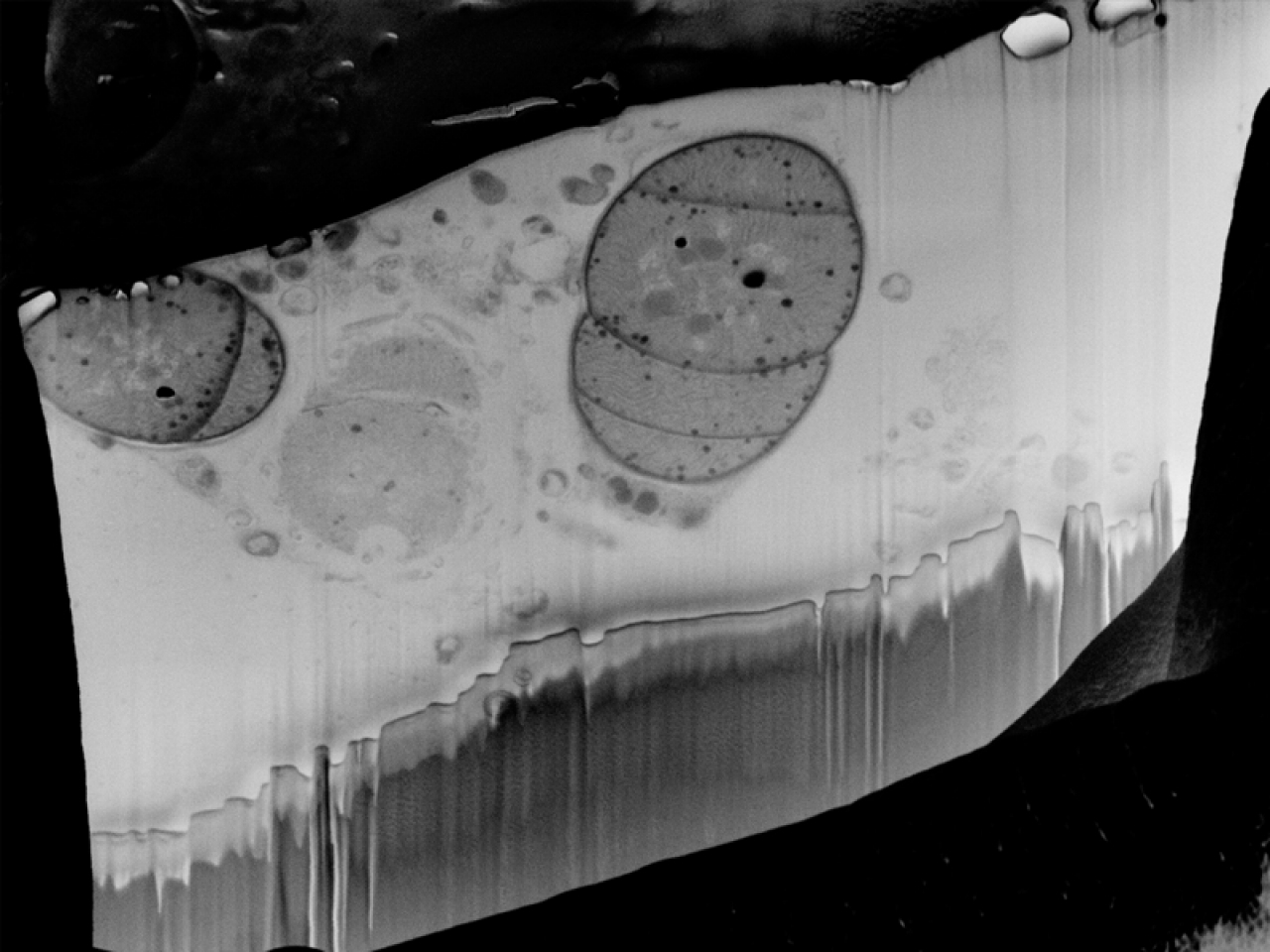
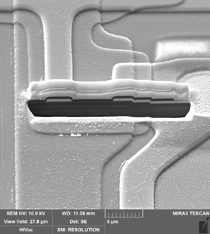
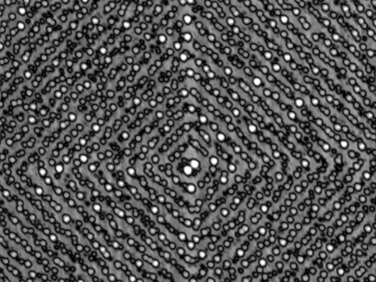
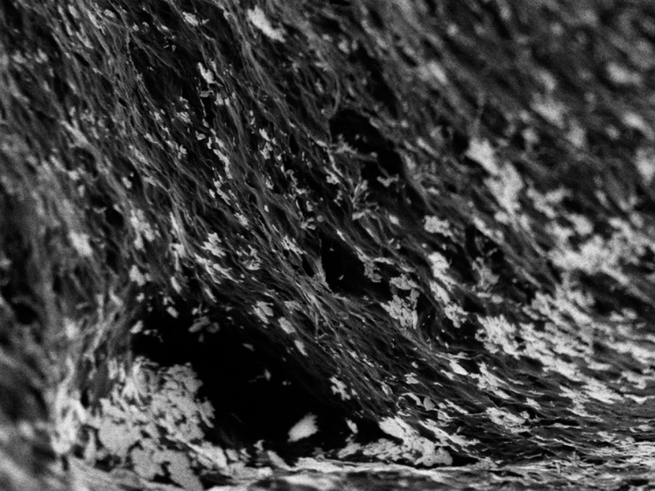
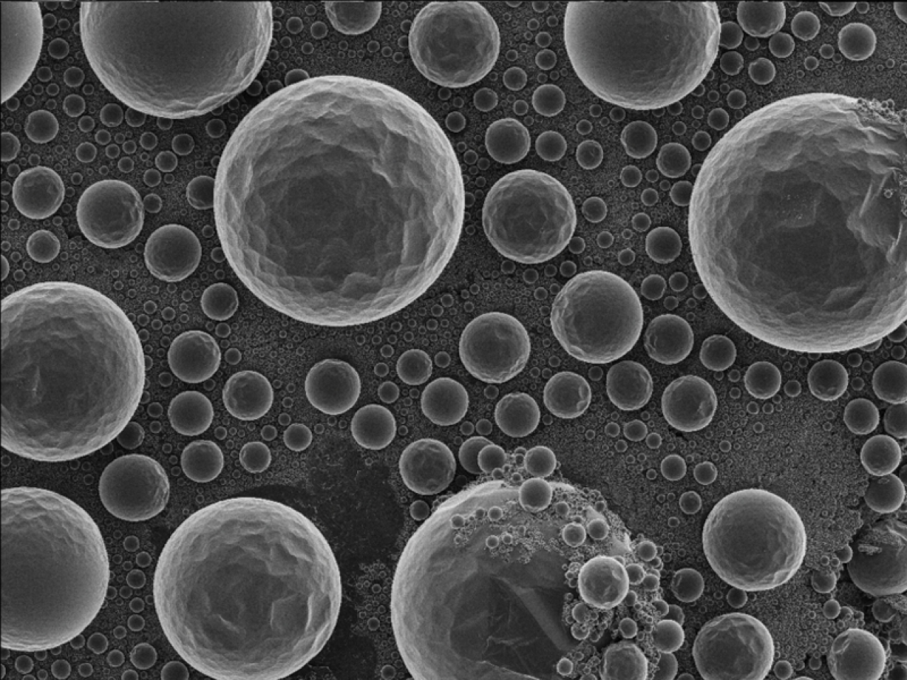
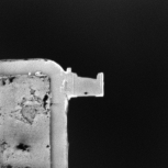
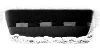
  • Cross-section of the sample without deposition @85 nA did not induce curtainings (FOV = 85 μm)

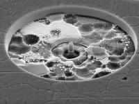
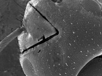
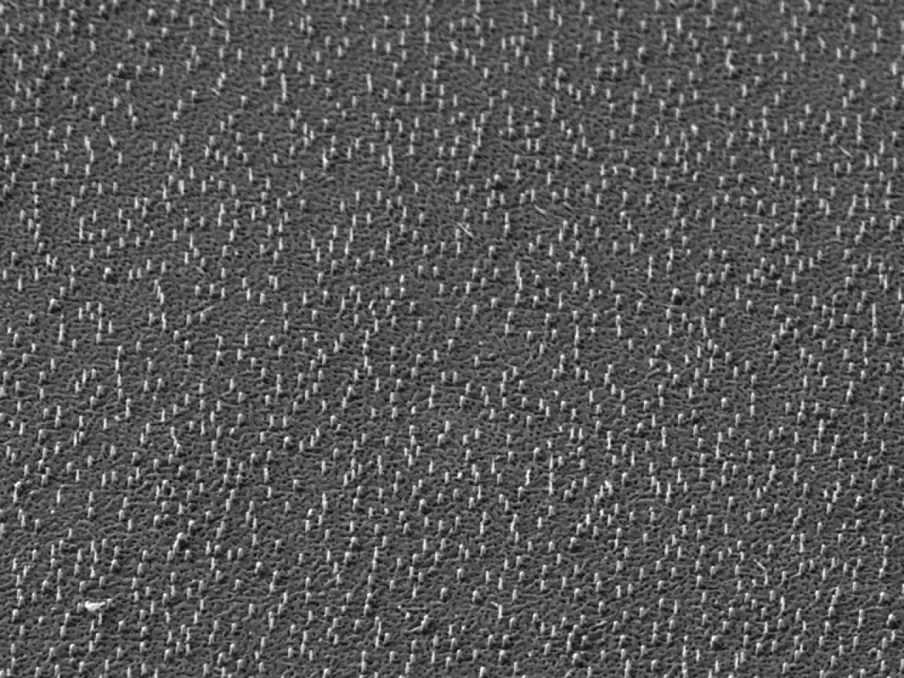
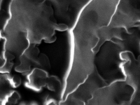
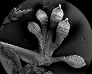
  • A large field of view of 1 mm allows to locate a specific area, here on a Gecko leg


i-FIB+

50 times faster than
the most powerful Ga FIB
With i-FIB+, save an hour every minute

i-FIB+ column is the perfect answer for today’s low machining time growing demands. With the patented compact no cooling ECR source technology, i-FIB+ achieves a sputtering rate up to 50 times higher than the most powerful Ga FIB keeping sharp current distribution. These assets are well adapted for sub-100 nm thickness samples preparation required for high-quality TEM images. Not only has i-FIB+ the great asset to get rid of gallium primary ions thanks to the use of non-contaminant noble gas ions non-contaminant for microelectronic processes, but also it is able to deliver probe current up to 3 µA making the milling of large structure much more time effective. The column allows the preparation of large-area cross-sections, as large as 1mm wide at 30 keV, that is unmatched in the market.

  Key Features

  Source

  Compact Plasma Ion Source ( 2.45 GHz HF
  Electron Cyclotron Resonance technology)

  Ion Species

  Xe+ / Ar+ / N2+ / He+ / O2+

  Energy Range

  3 - 30 keV

  Probe Current (with Xe+)

  1 pA – 3 µA

  Optimal Working  Distance

  12 mm

  Optional UHV  Configuration
  Maximum bakeout temperature is 120 °C


  • Ant head slices performed with i-FIB (FOV = 690 µm)

  • Cross section of MEMS sample using i-FIB on a TESCAN FERA3 (FOV = 125 µm)

  • Nano-pillar prepared with i-FIB on a TESCAN FERA3 (FOV = 274 µm)

  • SEM image of very large TEM lamella prepared with Xe i-FIB on TESCAN FERA3 (FOV = 270 µm width)


Orage

Extended performances with our new Ga FIB column

Orage is our very last Ga FIB column released. While keeping the well-proven performances of Cobra, Orage extends the panel of applications thanks to both an optimized design for low energy work and a sharply focused beam even for high currents. The addition of a piezo-controlled motor source gives an excellent FIB characteristic reproducibility and ease-of-use regardless of energy or current applied.

  Key Features

  Source

  LMIS (Liquid Metal Ion Source)

  Ion Species

  Ga+

  Energy Range

  500 eV - 30 keV

  Probe Current

  1 pA - 100 nA

  Working Distance

  12 mm

  Optional UHV Configuration

  Maximum bakeout temperature is 120 °C

  • Cross-section of resin-embedded cyanobacteria using Orage FIB coupled with TESCAN LYRA3 SEM (FOV = 20 µm)

  • Serial preparation of TEM lamellae using Orage FIB coupled with TESCAN LYRA3 SEM (FOV = 90 µm)

  • Cross-section in polymer nanofibers using Orage FIB coupled with TESCAN LYRA3 SEM (FOV = 50 µm)

  • Cross-section of Al bonding wires obtained with Orage FIB and TESCAN LYRA3 SEM (FOV = 250 µm)


Cobra

The well-recognized Ga FIB column

With an ultimate beam resolution of 2.5 nm, Cobra is the finest Gallium column. Cobra is designed to keep an extremely well-defined beam shape at different current modes. This well-approved FIB column allows both unique milling performances and imaging capabilities. Cobra FIB column is serially set up on mostly FIB-SEM instruments even for UHV atmospheres.

  Key Features

  Source

  LMIS (Liquid Metal Ion Source)

  Ion Species

  Ga+

  Energy Range

  1 - 30 keV

  Probe Current

  1 pA - 50 nA

  Working Distance

  12 mm

  Optional UHV Configuration

  Maximum bakeout temperature is 120 °C


  • Several metal lines FIB-cuts for circuit edit (FOV = 35 µm)

  • Nano-pillar prepared with Cobra for micro-mechanical tests

  • TEM lamella prepared with Cobra

  • Nano-pillar prepared with Cobra for micro-mechanical tests (TESCAN LYRA3) (FOV = 35 µm)

  • Cross-section of metal contacts and data lines in TFT (Thin-Film Transistor) array using Cobra FIB and TESCAN MIRA3 SEM (FOV = 30 µm)


Cobra ExB

High resolution Ga-free FIB column

Cobra ExB is a specific FIB column providing a performing alternative to the well-known Cobra FIB (gallium source). Thanks to the alliance of a LMAIS (Liquid Metal Alloy Ion Source) and a Wien Filter, Cobra ExB offers an easy solution for ion mass selection from light species to heavy clusters with great resolution imaging. This Ga-free FIB Column achieves precise milling and accurate selective surface implantation with a large panel of ion species.

  Key Features

  Source

  LMAIS (Liquid Metal Alloy Ion Source)
  AuGe / AuSi / Bi / Ga

  Ion Species

  Au+, Au++, Au2+, Au3+, Ge+, Si+, Si++, Gold clusters (Aunq+ 
  with n/q up to 100), Bi+, Bi++ ,…

  Energy Range

  1 - 30 keV

  Probe Current

  1 pA - 20 nA

  Characteristics

  High mass resolution ExB Wien Filter
  with 12 movable acceptance apertures
  (M/ΔM > 45)

  Miscellaneous   Alternative LMAIS can be available upon request


  • AFM image of Au nanocatalyst by FIB local implantation (50 nm spot size) using Cobra ExB

  • Observation of an AFM tip (x5000) using Cobra ExB and TESCAN LYRA1 SEM

  • Self-organization of Ge nanocrystals (50nm) by FIB dewetting using Cobra ExB

  • Nanowires vertical growth with gold droplets as catalysis (FOV = 83 µm)


Chroma ExB

Pentode objective for ultimate
performances in Ga-free environment

Chroma ExB FIB column introduces an all-new objective design called “pentode” for optimizing both low and high current modes in one single device. The association of a LMAIS and a Wien Filter reaches accurate ion mass selection from light species to heavy clusters keeping extreme resolution imaging due to the pentode objective. This Ga-free primary beam achieves especially precise milling, low energy range working and selective implantation with a very large panel of ion species.

  Key Features

  Source

  LMAIS (Liquid Metal Alloy Ion Source)
  AuGe / AuSi / Bi / Ga

  Ion Species

  Au+, Au++, Au2+, Au3+, Ge+, Si+, Si++, Gold clusters
  (Aunq+ with n/q up to 100), Bi+,Bi++,…

  Energy Range

  500 eV - 30 keV

  Probe Current

  0.1 pA - 50 nA

  Characteristics

  High mass resolution ExB Wien Filter
  with 30 movable acceptance apertures
  (M/ΔM > 45)

  Miscellaneous

  Alternative LMAIS can be available upon request

  • Graphene sample observed with Chroma ExB (view from the side) (FOV = 100 µm)

  • Graphene sample in another view using Chroma ExB (FOV = 200 µm)

  • Chroma ExB installed on NanoSpace FIB-SEM instrument

  • Observation of a molybdenum sample with Au+ primary ions (AuGe LMAIS)


Taipan

Unique correlative Optical / FIB column

Featuring patented coaxial technology, Taipan column achieves simultaneously optical and FIB images offering a wide range of applications such as circuit edit (CE), biology, biotechnology and ion beam lithography. Nondestructive photon imaging coupled with high resolution ion milling give the opportunity to reach new specifications for advanced 3D reconstruction and retro-engineering processes.

Its innovative compact objective lens design allows to obtain the smallest spot size keeping an excellent photon resolution. Taipan could be also available in a correlative electron / photon column configuration.

 Key Features

  Source

  LMIS (Liquid Metal Ion Source)

  Ion Species

  Ga+

  Energy Range

  15 - 30 keV

  Probe Current

  Application in nanotechnology  0.25 pA - 20 nA

  Working Distance

  From 5 mm (high resolution)  to 14.1 mm
  (optical correlation)


  • Microchip optical image obtained with Taipan coaxial ion/photon column (FOV = 200 µm)

  • Tin balls on carbon plate image performed with Taipan (FOV = 25 µm)

  • Tin balls on carbon plate image performed with Taipan (FOV = 66 µm)

  • Backside optical image of a silicon device obtained with Taipan coaxial ion / photon column with wavelength 1000 nm (FOV = 200 µm)