World leader in customized focused ion and electron beam technology
Scientific Overviews
Why using a FIB?
The Focused Ion Beam (FIB) column is an optical instrument which focuses and scans an accelerated ion beam on a sample in a vacuum chamber. Such a column can be used for two main purposes:
- To form scanning ion images by collecting the secondary electrons (SE) generated by the interaction of the incident ions and the sample surface.
- To locally sputter the material surface to directly fabricate arbitrary nanostructures.
The most commercially available FIB systems are using gallium (Ga) ions for micromachining of the surfaces.
During the last 25 years, FIB instrumentation has become a key technology for wide fields of materials science applications, from circuit editing to Transmission Electron Microscopy (TEM) sample preparation, microstructural analysis and prototype nanomachining. Associated with a SEM (Scanning Electron Microscope), FIB instruments have become a powerful tool for nano-manipulation and nano-fabrication when coupled with micromanipulators. Equipped with a Gas Injection System (GIS) nanometric local deposition (using the GIS) can even be obtained.
The basic functions of the FIB, namely, imaging and sputtering with an ion beam (meaning milling or etching), require a highly focused beam for high resolution (see fig. 1). A consistent theory of any focused beams state that the smaller the effective ion source size, the more current can be focused in a single probe.
Liquid Metal Ion Source (LMIS) is used in most of commercial and academic systems designed for micromachining applications (see fig. 2). These sources are point sources based on field emission to produce the ions. Their brightness is several orders of magnitude higher than any other type of other sources. Therefore, unlike plasma ion sources, LMIS have a small virtual source size of the order of 50 nm suitable to focus the ions in a spot of few nanometers.
LMIS are able to provide several ion species, with the most widely used being a Ga-based blunt needle source. Ga has decided advantages over other metals such as In, Bi, Sn, and Au because of a nice combination of low melting temperature (30°C), low vapor pressure and reasonable wetting of tungsten needles. The low melting temperature makes the source easy to design and operate at room temperature. As gallium does not react with the material the needle is typically made of tungsten (W) and evaporation is negligible. Ga-based LMIS have typically the longest lifetime and are the most stable LMIS. These last points are crucial for ultra-high resolution and long lasting time work.
During operation, gallium ions flow from a reservoir to the needle apex and a large negative voltage is applied between this needle and an extraction electrode. The balance between the electrostatic forces and the surface tension of gallium wetting the tapered W needle geometry results in the formation of a typical shape of the liquid, named Taylor cone with a half angle of 49.3° (see below fig. 3). For a typical emission current of 2µA, the cone is distorted and a cusp is formed at the apex of the Taylor cone with a diameter of approximately 5 nm (see fig. 4). At the apex of this cusp the electric field is of the order of 1.5x10¹⁰ V/m sufficient to extract the ions by field emission.
 Figure 3. The Taylor cone and the ion emission at the apex by field emission
The simplest and most widely used ion beam column design consists in two lenses (namely a condenser and objective lens) to focus the ion beam on the sample, a beam-defining apertures to select the beam diameter and probe current, deflection plates to raster scan the beam over the sample surface, an octupole stigmator to ensure a circular beam shape, a high-speed beam blanker to quickly deflect the beam off the sample and a Faraday cup to measure the ion current available (see below fig. 5). A ExB mass filter can be added in the case of alloy LMIS (called LMAIS for Liquid Metal Alloy Ion Source).
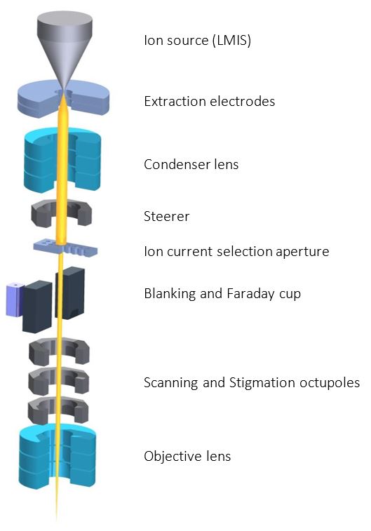
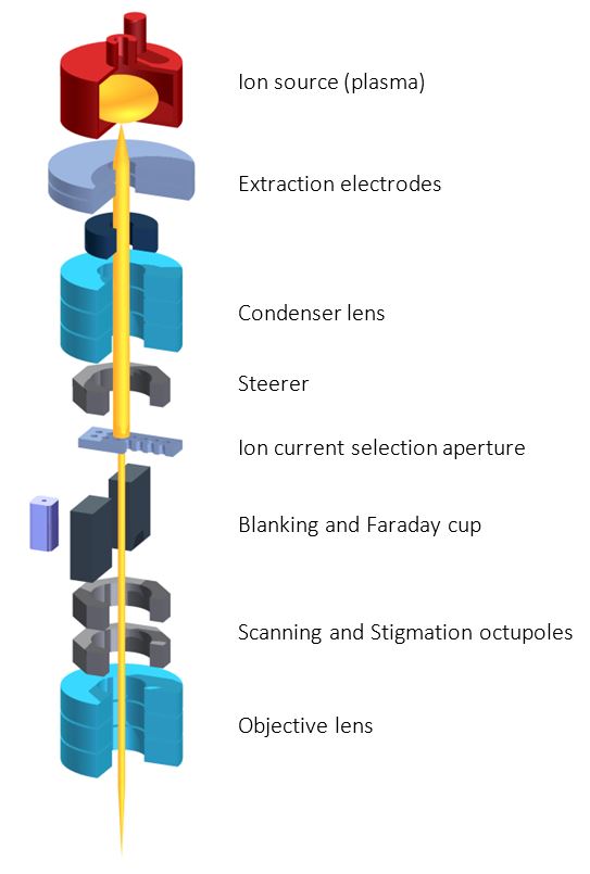
Figure 5. FIB column schematic (left: LMIS / right: plasma source)
The beam current profile of on the sample determines the imaging resolution and micromachining precision. Generally, the smaller the beam diameter, the better the achievable resolution and milling precision. However the requirements for both applications are not exactly the same. For the energies, currents, and acceptance angles used in typical FIB systems, the beam spot size is limited mostly by the chromatic aberration that results primarily from the energy spread of the ion source. This energy broadening is due to space charge effects at the ion source and secondarily from additional broadening in ion crossovers in the column. At higher current the main limitation is the spherical aberration which induces large tails in the ion spot.
With only ions, FIB is only a subtractive method where material is removed from the sample. To transform the system into an additive method, a GIS which locally delivers an organometallic gas is an efficient method to deposit material on the surface. In addition using a suitable reactive gas, it is possible to enhance the etching rate or do in site-specific CVD (Chemical Vapor Deposition). In term of deposition process, secondary electrons generated by the primary ion beam (or, alternatively, the incident electron beam in dual-beam FIB-SEM systems) can crack hydrocarbon precursor gases, leading to local deposition of a conducting (W, Pt, C…) or insulating material (SiOx) (see below fig. 6).
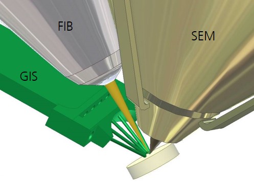 Figure 6. Dual Beam FIB-SEM apparatus coupled with GIS
Introducing a micromanipulator in the chamber with the local deposition of material also enables sophisticated operations within the FIB system, which transform the FIB instrument in a nanofabrication unit (see fig. 7).
The ultimate system is obtained by gathering a FIB column, a GIS to add and remove material, a micromanipulator to move in-situ the created objects and a SEM to observe the operations at high resolution and in real time without any material removal.
Ion-solid interactions play an important role in a wide range of different endeavors, ranging for example from fabrication of microelectronic devices to understanding the distributions of cosmic gases. An ion impinging a solid loses its kinetic energy through binary collisions with the atoms of the sample. This transfer of energy from the ion to the solid results in a number of different processes:
- ion reflection and backscattering
- secondary electron emission
- electromagnetic radiation
- surface sputtering and secondary ion emission
- sample damage through ion cascades
- sample heating
Traditional detectors developed for SEM applications can be used to detect the secondary electrons or x-rays created by the interaction of the ion beam with the sample. The ions sputtered from the sample can also be detected using a variety of detectors such as charge electron multipliers. Mass selection of the sputtered charged particles is also possible (SIMS Secondary Ion Mass Spectrometry) to provide elemental analysis capabilities.
Conventional SEM imaging is based on detecting the Secondary Electrons (SE). Today most imaging method in FIB is based on detecting the low-energy electrons, often referred as Ion-induced Secondary Electrons (ISE). Images obtain from scanning ion microscopy exhibit a better contrast than from SEM’s as they are more sensitive to the atomic number. The electron yield depends also strongly on surface oxidation and contamination and thus will change as the surface is sputtered and cleaned with the incorporation of gallium.
Up to now, focused Ion Beams spot deliver images with lower resolution than scanning electron microscopes. However, ISE imaging typically delivers stronger channeling contrast from crystals than SE imaging. The contrast due to crystal orientation is easily detected from material contrast, as crystal contrast changes with the incidence angle of the ion beam and material contrast does not.
Finally FIB is a powerful tool for nanomachining of 3D patterns either by removing or adding material on surfaces. Associated with advanced ion detectors and filters it provides elemental analysis at very small scales. Adding also a micromanipulator it becomes a nanofabrication factory. New ion source concepts such as ultra-cold atoms or plasma sources should go further in term of ultimate resolution and sputtering yield in the near future.
The video below presents the whole TEM sample preparation procedure using a TESCAN LYRA3 dual beam FIB-SEM platform (Cobra FIB) equipped with a GIS (5-line GIS) and a micromanipulator:
Reference:
Focused Ion Beam Microscopy and Micromachining C.A.Volkert and A.M. Minor
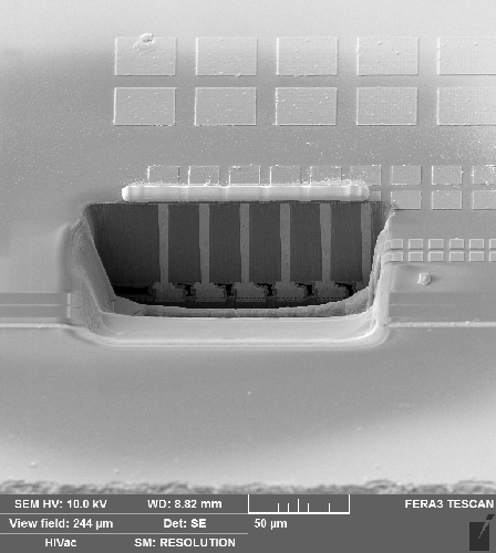
Figure 1. Cross-section micromachining using FIB
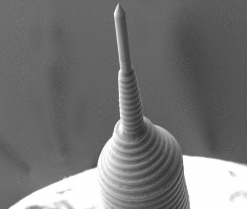
Figure 2. Picture of a LMIS
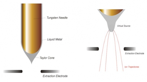
Figure 3. The Taylor cone and the ion emission at the apex by field emission
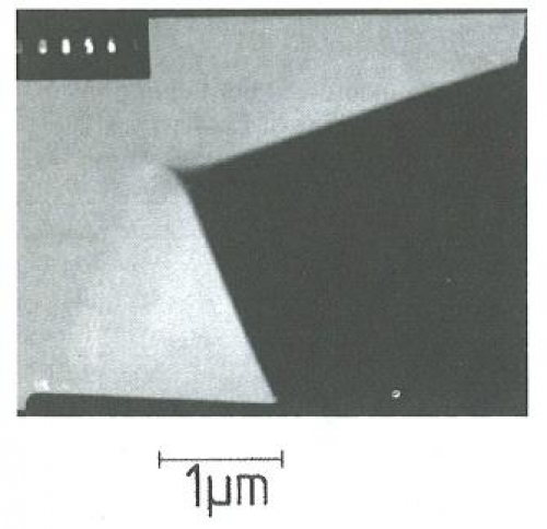
Figure 4. TEM image of operating LMIS source - Dr G. BenAssayag and Dr P. Sudraud experiments carried out on a 3 MeV TEM revealed that the cone apex is elongated in a thin liquid jet which is the starting point of the ion emission
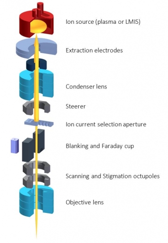
Figure 5. FIB column schematic
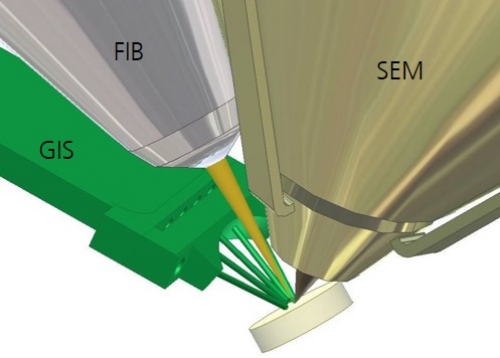
Figure 6. Dual beam FIB-SEM apparatus coupled with GIS
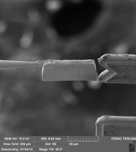
Figure 7. TEM sample preparation using plasma FIB (i-FIB), GIS and a micromanipulator on a TESCAN FERA3 dual beam FIB-SEM platform