World leader in customized focused ion and electron beam technology
Scientific Overviews
Why using a SEM?
The different signals available from the electron beam interaction with atoms are at various depths within the sample. In the most common or standard detection mode the secondary electron coming just below the surface are collected. The number of secondary electrons that can be detected depends on the angle at which beam meets surface of specimen, i.e. on specimen topography. Consequently, SEM can produce very high-resolution images of a sample surface, revealing details less than 1 nm in size of the surface topography.
Back-Scattered Electrons (BSE) are incident electrons that are reflected from the sample by elastic scattering. They emerge from deeper locations within the specimen and consequently the resolution of BSE images is generally poorer than SE images. However, BSE are often used in analytical SEM along with the X-rays analysis because the intensity of the BSE signal is strongly related to the atomic number of the specimen. BSE images can provide information about the concentration of different elements in the sample. For the same reason, BSE can image colloidal gold immuno-labels of 5 or 10 nm diameters, which would otherwise be difficult or impossible to detect in secondary electron images in biological specimens.
Characteristic X-rays are also emitted when the electron beam removes an inner shell electron from the sample, causing a higher-energy electron to fill the shell and release energy. These characteristic X-rays are used to identify the composition and measure the abundance of elements in the sample. This related technic is called Energy-Dispersive X-ray Spectroscopy (EDS, EDX, or XEDS).
The SEM spreads out in all fields that require characterization of solid materials. While this contribution is most concerned with geological applications, it is important to note that these applications are a very small subset of the scientific and industrial applications that exist for this instrumentation. For fast characterization in many applications SEM operation requires minimal sample preparations.
Compared to the early beginning Modern SEM's are easy to operate, with user-friendly "intuitive" interfaces. For many applications, data acquisition is fast (less than 5 minutes/image for SE, BSE, spot EDS analyses.) These SEM generate data in digital formats, which are highly portable and can be numerical easily treated. But an electrically conductive coating must be applied to electrically insulating samples for study in conventional SEM, unless the instrument is able to operate in a low vacuum mode.
Samples must be solid and fit into the microscope chamber. Maximum size in horizontal dimensions is usually on the order of 10 cm, vertical dimensions are generally much more limited and rarely exceed 40 mm. For most instruments samples must be stable in a vacuum on the order of 10-5 - 10-6 Torr. However for microelectronics applications large chamber are existing and available for 300-mm wafers.
Samples likely to outgas at low pressures (rocks saturated with hydrocarbons, "wet" samples such as coal, organic materials or swelling clays, and samples likely to decrepitate at low pressure) are unsuitable for examination in conventional SEM. However, "low vacuum" and "environmental" SEM also exist, and many of these particular samples can be successfully examined in these specialized instruments.
For elemental analysis, EDS detectors on SEM cannot detect very light elements (H, He, and Li). Most SEM are using a solid state X-ray detector (EDS), and while these detectors are very fast and easy to utilize, they have relatively poor energy resolution and sensitivity when compared to wavelength dispersive X-ray detectors (WDS) on most Electron Probe Micro-Analyzers (EPMA).
As a complementary ability for SEM, Focused Electron Beam Induced Deposition (FEBID) is a direct-writing technique with nanometer resolution, which has received strongly increasing attention within the last decade. In FEBID a precursor is injected using a Gas Injection System (GIS). The open end of the capillary is brought into close proximity to the substrate surface on which the electron beam is focused. The gas is adsorbed on a substrate surface and then dissociated by the focused electron beam. The beam, which can be sub-nanometer in modern electron microscopes, deposits 2D or 3D nano- to micrometer-wide structures with a high precision. Micro-devices can be rapidly prototyped. Applications have already been found as a quality control tool for finding and repairing defects in computer chips and lithography masks. Other applications are electrical contacts between single bio-molecules or nano-wires for basic research, fabricating miniaturized 3D devices and high-resolution contact scanning probes. These tools are complementary to Focused Ion Beams (FIB).
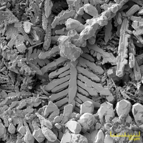
Figure 1. Observation of Ag crystals from electrolysis with TESCAN MIRA3 SEM
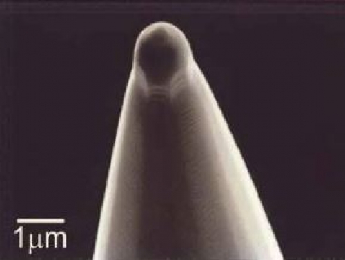
Figure 2. Picture of a Schottky emitter (from www.denka.co.jp)