World leader in customized focused ion and electron beam technology
Scientific Overviews
Why using a GIS?
A Focused Ion Beam (FIB), when scanning a given area, modifies the sample surface in different ways depending on the energy of the incoming ions. By only irradiating in the typically used 5 - 30 keV energy range, the exposed area is principally etched as a consequence of mechanical collisions between accelerated ions and surface atoms. Higher energies and low currents (> 50keV) are used to implant deep the primary element of the beam in the sample, whereas low energies (some keV - few eV) induce surface amorphization, implantation, or imaging without too high alteration.
The surface interaction of the ions with the surface generates local energy by activating the exposed area and also by inducing secondary electrons. All this energy can be used to create a surface reaction by introducing locally some chemistry thanks to an injection system called GIS (Gas Injection system). The chemical is injected in the gaseous form but can be originally solid, liquid, or already a gas. This opens a wide range of possible applications mostly separated into 2 main directions:
- the deposition to create micro or nanostructures
- the control of the milling rate of the surface
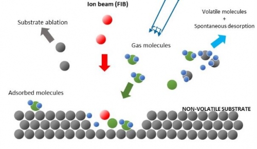
These two processes can be observed when using a FIB but also a FEB (Focused Electron Beam). The amount of energy when using the FIB generally enhances the reaction kinetics but also allows to produce more compounds at the surface. Nevertheless, compared to SEM-based induced reactions, when using the FIB, the induced milling due to the impact of the ions with the surface have to be taken into account in the reaction the user wants to make. The basic principle of this method is the introduction of a vapor containing some suitable chemical form of the desired material into the sample chamber. Molecules from the gas are adsorbed at the surface due to Van Der Waal’s forces. The energy brought by the beam then dissociates these molecules modifying the scanned area. It is generally accepted that the secondary electrons produced by the collision of the ions or primary electrons with surface atoms are involved in the cracking of the adsorbed precursor molecules. These secondary electrons possess low energy (<50 eV) comparable to the classical molecules’ bond energies responsible for the cracking of the precursor or the formation of bonds between chemicals and surface atoms.
Two main reactions are generally observed when introducing chemical molecules: surface etching modification or material deposition.
With a gas that could produce volatile molecules with the surface, the mechanical etching due to the focused beam can be controlled (enhanced or lowered) due to local chemical reactions. On one hand, when volatiles by-products are formed, the sputtering rate is increased and less material redeposition is observed. On the other hand, harder layers can also be created near the area exposed and a diminution of the sputtering rate can be achieved. Nevertheless, some samples can present various configurations and various surface elements. In this particular case, the FIB milling becomes heterogeneous because of the difference in etching rates of all the surface elements. As an example, the surface of an IC chip presents lines of metal embedded in dielectric. In this case, the chemistry can help to remove the selectivity of the FIB milling by introducing the proper elements in the region of interest.
With some other gases, the decomposition of the adsorbed molecules by FIB or SEM results in a local deposition of material. The secondary electrons can break the chemical bonds of the adsorbed molecules and dissociate the initial precursor into different components: volatile ones pumped away from the chamber and others not volatile that would remain deposited creating nanopatterned geometries.
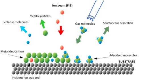
Ion-induced processes using a gas injection system to introduce precursor near the sample surface. On the left image is presented an injection of organometallic precursor inducing the deposition process. On the right image, the gas introduced helps to enhance the milling of the sample surface.